


- News
12 December 2018
Powering up gallium oxide metal-oxide-semiconductor field-effect transistors
Hebei Semiconductor Research Institute and Institute of Microelectronics in China claim record power figure of merit performance for β polymorph gallium oxide (β-Ga2O3) metal-oxide-semiconductor field-effect transistors (MOSFETs) [Yuanjie Lv et al, IEEE Electron Device Letters, 14 November 2018].
The 50MW/cm2 figure of merit represents a high breakdown voltage combined with a low on-resistance. High performance of one or the other factor usually entails a reduced characteristic on the other side of the trade-off.
The high figure of merit was achieved by using a source-connected field plate to reduce peak electric fields, increasing breakdown performance. Ion implants in the source and drain regions of the devices reduced contact resistance to 1.0Ω-mm.
The wide 4.5-4.9eV bandgap of β-Ga2O3 suggests that a high critical electric breakdown field of order 8MV/cm is possible in the material. In theory it should be possible to reach a power figure of merit in the range 34,000MW/cm2, so there is clearly much scope for development and optimization work. Before the Hebei/Institute of Microelectronics work the highest reported power figure of merit was 10MW/cm2.
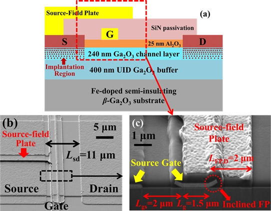
Figure 1: (a) Schematic cross section of source-field-plated β-Ga2O3 MOSFET, and scanning electron microscope images of (b) surface and (c) cross section of device.
The substrate for metal-organic chemical vapor deposition (MOCVD) was iron-doped semi-insulating (010) β-Ga2O3. The precursors were trimethyl-gallium and oxygen delivered at 8Torr pressure. The substrate temperature was 750°C. Silicon (Si) doping for the 240nm n-type channel layer (Figure 1) was provided by silane (SiH4) flow. Van der Pauw measurements gave an electron density of 1.95x10¹³/cm2 with 90cm2/V-s mobility, giving a sheet resistance ~3.6kΩ/square.
Inductively coupled plasma (ICP) etch was used to give a 350nm-high mesa for device fabrication. Source and drain regions were created with multiple implantations of silicon ions to a depth of ~210nm. Simulations predicted that the surface silicon concentration would be around 1020/cm3. After annealing the doping implants, Ohmic source/drain (S/D) contacts were formed with the deposition of titanium and gold. The gate (G) stack consisted of 25nm of 250°C atomic layer deposition (ALD) aluminium oxide (Al2O3) and nickel/gold metal electrode. The aluminium oxide was annealed before electrode deposition.
Surface passivation was provided by 400nm plasma-enhanced chemical vapor deposition (PECVD) silicon nitride (SiN). After reactive-ion etch to expose the source and drain metal, the nickel/gold source-connected field plate that extended 2µm toward the drain was formed.
The 1.5µm-long gate was 40µm wide. The gate-source distance was 2µm. Devices with gate-drain spacings of 7.5µm and 14.5µm were fabricated. The respective source-drain distances were 11µm and 18µm.
With the gate at 5V, the saturation drain current was 267mA/mm for the 11µm source-drain device and 222mA/mm for the 18µm version. Under the same gate potential, the low drain bias on-resistance was 41.6Ω-mm in the 11µm source-drain transistor.
With 20V drain bias, the maximum transconductance for the 11µm MOSFET was 10.5mS/mm. The 0.1mA/mm threshold gate voltage was at 50.5V. Gate leakage was around 7.1x10⁻⁷A/mm. The researchers see this value as being “comparatively large”, adding that the culprit may be Al2O3/Ga2O3 interface traps. They suggest that these traps could be reduced with a better optimized surface-state treatment. Further evidence of interface traps was given by ~0.8V hysteresis in the response under forward and reverse sweeps of gate voltage. The on/off current ratio was of the order 106.
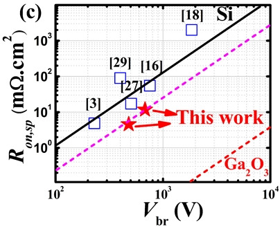
Figure 2: Three-terminal off-state breakdown characteristics of β-Ga2O3 MOSFET with and without source-field plate for (a) 11µm and (b) 18µm source-drain distance devices. (c) Plot of Ron,sp versus Vbr for Hebei/Institute of Microelectronics devices (“this work”) and other reported lateral Ga2O3 MOSFETs.
Destructive breakdown performance in air was carried out with the gate at -55V (Figure 2). Without source field plates, the breakdown voltages (Vbr) were 310V and 260V for the 18µm and 11µm MOSFETs, respectively. These values were greater than the 218V value expected from a one-sided abrupt-junction model. The researchers suggest that the better-than-theory result is due to non-uniformity of channel doping and depletion from interface states. Adding source field plates increased the breakdown to 480V in the 11µm device and 680V in the 18µm MOSFET.
Multiplying the on-resistance by the source-drain distance to give a specific on-resistance (Ron,sp), the researchers found values of 4.58mΩ-cm2 and 11.7mΩ-cm2 for the 11µm and 18µm devices, respectively. “Our fabricated devices in this work show much lower Ron,sp compared with other β-Ga2O3 MOSFETs and also with the theoretical performance of Si-based power devices,” the team comments.
The power figure of merit given by Vbr2/Ron,sp was thus 50.4MW/cm2.
Although the saturation drain current is still lower than in reported nanomembrane Ga2O3 devices, the researchers claim that their source-field-plated MOSFET shows a record maximum drain current and power figure of merit among devices fabricated on homoepitaxial β-Ga2O3. The researchers suggest that increasing the channel layer thickness in conjunction with gate recessing could lead to lower on-resistance and associated improvement in the power figure of merit.
Gallium oxide metal-oxide-semiconductor field-effect transistors MOSFETs
https://doi.org/10.1109/LED.2018.2881274
The author Mike Cooke is a freelance technology journalist who has worked in the semiconductor and advanced technology sectors since 1997.


