


- News
16 August 2018
SMI optimizes NanoV CVD research reactor for SiGeSn growth
© Semiconductor Today Magazine / Juno PublishiPicture: Disco’s DAL7440 KABRA laser saw.
Structured Materials Industries Inc (SMI) of Piscataway, NJ, USA – which provides chemical vapor deposition (CVD) systems, components, materials, and process development services – has optimized a design version of its NanoV CVD research reactor for exploring growing thin films of silicon germanium tin (SiGeSn) materials.
The NanoV CVD research system is configured for growth on single 2” wafers, but a 3” platter is also available. Advantages of the 2” substrate reactor include its optional height-adjustable water-cooled showerhead, the substrate susceptor rotation, an upgradeable option to include a double wall for very high-temperature operation, and plasma enhancement.
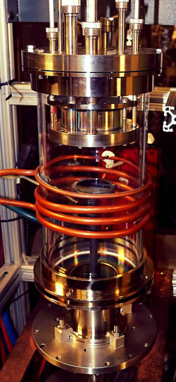 Picture: SMI’s in-house NanoV CVD reactor with a 2" wafer platter in place.
“The height-adjustable showerhead is an important feature for some researchers since it changes the distance between gas injection and substrate and, thus, gas-phase pre-reaction pathways,” notes research scientist Dr Arul Arjunan. “SMI designed a height-adjustable modular showerhead to allow exploration of these effects (along with rotation) with different chemistries,” he adds. “The showerhead modification allows the showerhead-to-susceptor distance to be adjusted to determine the best position for a given set of process parameters as well as tune the pre-reactions, efficiency, and uniformity.”
The NanoV CVD system for SiGeSn growth also optionally features substrate rotation through the SMI SpinCVD rotation assembly. Substrate rotation helps to improve uniformity and efficiency as well as to minimize pre-reactions. At high speed (several hundred rpm), rotation generates forced convection, which can be used to enhance laminar flow and thus uniformity and efficiency.
The plasma-enhancement option can catalyze low-temperature cracking of the precursors, provide radicals to enhance reaction pathways, and enhance surface atom mobility, all of which are important for the growth of SiGeSn. SMI offers a low-cost unregulated 180–250kHz output frequency 1kW power scale plasma option (that can generally operate through several tens of Torr) or a high-end 13.56MHz 300W plasma source option (that operates in the range from mTorr to a few Torr).
These tool developments have been supported in part by the US Department of Energy (contract no. DE-SC0015164), wherein SMI is funded to develop SiGeSn-based IR photodiode sensors and waveguides on silicon chips. That work is supported by a subcontract with professor Hongbin Yu of Arizona State University.
The NanoV CVD tool is a vertical reactor system designed to provide the researcher with the most complete and versatile low-cost CVD platform on the market to investigate of the widest range of materials and amorphous films and structures such as epitaxy, polycrystalline, or nanowires and nanotubes. This one platform is conveniently configurable for either oxidizing or reducing environments. Simple exchangeable components in a small footprint at an economical price allow the researcher great process variability – allowing great flexibility in adapting to changing research needs or supporting multiple material research needs on one simple platform with low-cost, modular, easily reconfigured components.


