


- News
9 August 2018
Integrating capacitors into p-gallium nitride gate transistors on silicon
Hong Kong University of Science and Technology (HKUST) and Taiwan Semiconductor Manufacturing Company Ltd have been jointly developing integrated capacitors for p-type gallium nitride (p-GaN) gate high-frequency power transistors on silicon substrate [Gaofei Tang et al, IEEE Electron Device Letters, published online 9 July 2018]. GaN transistors with a p-gate enable enhancement-mode operation where transistors are in the current-off state with zero gate potential. This reduces power consumption and allows fail-safe operation.
GaN transistors are being developed for high-frequency power applications with a view to high conversion efficiency and power density. Production on silicon should reduce manufacturing cost.
One problem with p-gate enhancement-mode transistors is parasitic inductance in the gate-drive loop causing over-voltage stress at high frequency. Parasitic inductance can be minimized by on-chip integration of high-voltage power switches and peripheral drive/control modules. Such integration is promoted by the availability of integrated passive devices – resistors and capacitors. Capacitors are used to help de-couple noise in the power supply, shift levels, and pump charge in the gate driver.
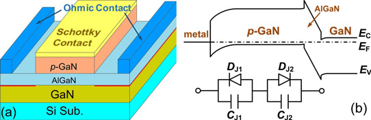
Figure 1: (a) Schematic cross section of fabricated p-GaN gate capacitor. (b) Schematic energy band diagram along depth of gate stack at zero bias and corresponding equivalent circuit.
The material structure for the p-GaN gate capacitors was metal/p-GaN/AlGaN/GaN produced for commercial 650V enhancement-mode power devices. The capacitor used ohmic contacts on the n-side and a Schottky contact on the p-GaN (Figure 1). The p-GaN material bends the underlying band structure upwards, depleting the two-dimensional electron gas (2DEG) that usually forms near the AlGaN/GaN interface, putting the device into an off-switch condition. The researchers modeled their device as back-to-back diodes consisting of the metal/p-GaN Schottky junction and the p-GaN/AlGaN/GaN heterojunction.
Above the threshold for formation of the 2DEG the Schottky diode capacitance is voltage-dependent while the heterojunction capacitance is considered as being voltage-independent. The heterojunction capacitance is dependent on the AlGaN barrier thickness. Below threshold the heterojunction capacitance is negligible, creating a low total capacitance, arising mainly from the fringe/edge regions.

Figure 2: (a) Measured C-V characteristics and extracted equivalent oxide thickness of p-GaN gate capacitor. (b) Measured gate leakage at varied temperatures under positive gate bias. (c) Extrapolated time evolution of gate voltage (VG) and current (IG) of charged p-GaN gate capacitor. (d) Calculated power consumption of p-GaN gate capacitor.
A 42μmx100μm rectangular device had a capacitance density of up to ~230nF/cm2 (Figure 2). The equivalent oxide thickness (EOT) of the stack ranged from 16nm to 20nm, with the respective voltage varying from 4V to 7V. The room-temperature DC breakdown was around 12.5V.
The gate leakage led to self-discharge from 6V to 5V in ~60μs and from 5V to 4V in ~500μs. The researchers comment: “Such a result suggests that the p-GaN gate capacitors are well suited for AC operation at frequencies above 100kHz (with a period less than 10μs).”
The gate-leakage-induced power consumption is calculated at ~30μW at 6V bias and ~4μW at 5V. “Such power consumption is negligible compared to the overall power consumption of the circuits (e.g. gate driver) featuring the capacitors,” the researchers comment. The gate-leakage was also found to increase with temperature.
The team suggests that operating voltages should be limited to less than 7V to avoid long-term stress-induced degradation.
The researchers also compared the performance of large-area 250μm-radius circular against interdigitated p-electrodes. The interdigitation consisted of six fingers measuring 54μmx360μm, giving comparable capacitance to the circular device. The aim was to suppress the distribution effect from series resistance to current flow in the 2DEG. The distribution effect limits operating frequency due to slow turn-on. The quality factor was 145 at 5MHz for the interdigitated capacitor, compared with 3.0 for the circular device.
Capacitors GaN p-gallium nitride gate transistors
https://doi.org/10.1109/LED.2018.2854407
The author Mike Cooke is a freelance technology journalist who has worked in the semiconductor and advanced technology sectors since 1997.


