


- News
16 August 2018
III-nitride solar cells on hexagonal boron nitride separation layer
Georgia Institute of Technology’s collaboration with France-based researchers in Metz has used hexagonal boron nitride (h-BN) as a separation layer for indium gallium nitride (InGaN) solar cells grown on sapphire [Taha Ayari et al, ACS Photonics, 30 July 2018].
After separation, the devices were transferred to glass with an aluminium (Al) back-reflector or a frequency-selective dielectric mirror. The hope is to hybridize the InGaN cell with other group IV and III-V cells, extracting power optimally from the solar spectrum in a lightweight, low-cost format.
The collaboration includes GT-Lorraine (http://lorraine.gatech.edu), GT-CNRS, (https://umi2958.gatech.edu), and Institut Lafayette (http://kippelengroup.gatech.edu/institut-lafayette).
Many techniques have been developed for separating III-nitride materials from sapphire growth substrates. Recently h-BN, a van der Waals bonded material, has been tried for light-emitting diodes and transistors. The GT-France researchers claim that their’s is the first attempt at using the technique for solar cells.
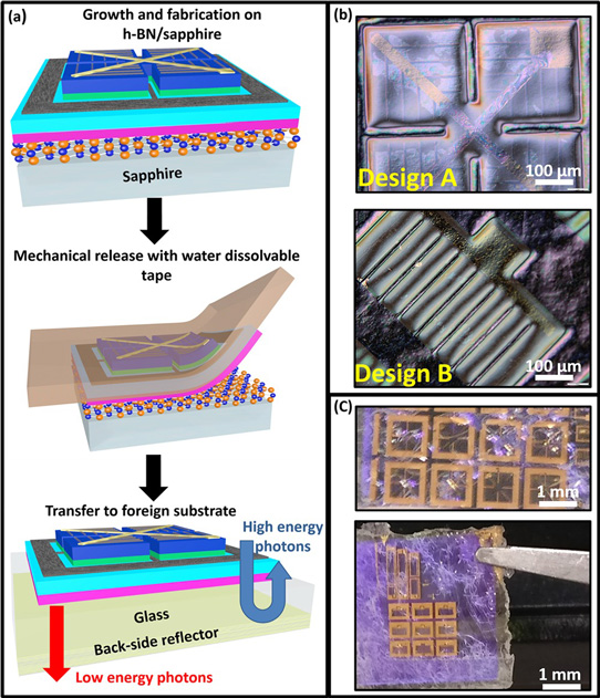
Figure 1: (a) Schematics of fabrication steps for releasing InGaN-based solar cells from sapphire and transfer onto foreign substrates. (b) Optical microscopy images from back side of ~ 1mm2 solar cells with two different designs on water-dissolvable tape after release. (c) Photographs of devices with different sizes and designs transferred to glass with dielectric mirror (purple background is due to reflected wavelengths between 375nm and 465nm).
The active structure consisted of 5x2.5nm In0.18Ga0.82N quantum wells (QWs) with 12nm GaN barriers grown on 3nm h-BN on 2inch-diameter sapphire using ‘van der Waals’ metal-organic vapor phase epitaxy (MOVPE).
Ammonia (NH3) was used as the nitrogen precursor, while triethylboron (TEB), trimethylgallium/triethylgallium (TMGa/TEG), trimethylindium (TMIn) and trimethylaluminum (TMAl) provided the metal sourcing. Silicon and magnesium doping for n-type and p-type GaN layers, respectively, came from silane (SiH4) and bis(cyclopentadiene)magnesium (Cp2Mg).
The h-BN was grown at 1300°C. The nucleation layer was 300nm silicon-doped 1100°C Al0.14Ga0.86N. The n-side of the device consisted of 0.5μm n-GaN; the p-side was 0.3μm p-GaN. The photoluminescence from the InGaN wells had a peak at 475nm.
The ‘van der Waals epitaxy’ refers to the base material h-BN, which has strong in-plane bonds but weaker ‘van der Waals’ forces keeping the hexagonal layers of BN sheets together. The weaker van der Waals bonds allow for easier damage-free separation from the sapphire substrate.
Fabrication involved plasma etching mesas and the deposition of titanium/aluminium/nickel/gold n- and nickel/gold p-contacts. Titanium/aluminium/nickel/gold was also used for bus bars.
The devices on sapphire under AM1.5 solar illumination conditions achieved 0.08% extracted efficiency, 39.5% fill factor, 1.17V open-circuit voltage and 0.17mA/cm2 short-circuit current density, comparable with the performance of conventional sapphire-substrate devices according to the team. The open-circuit voltage was lower than expected from simulations (2.28V) – the researchers suggest that this was mainly due to the difficulties in obtaining good ohmic contacts on p-GaN. The simulated efficiency was also higher at 0.14%.
The low sub-1% efficiency is due to the short-wavelength response, which does not cover much of the solar AM1.5 spectrum (roughly the spectrum viewed from the ground at 48.2° solar zenith angle suitable for mid-latitudes in summer).
Illumination with 440nm-wavelength light at 140mW/cm2 power density gave an open-circuit voltage of 1.6V and short-circuit current density of 40mA/cm2. The team comments: “These increased performances under high irradiance confirm the suitability of the InGaN solar cells for high concentrated photovoltaic (HCPV) applications.”
The devices were transferred to glass with a back-reflector. The transfer involved water-dissolvable tape and polyurethane resin as bonding. The technique enabled transfer intact without damage. The absence of harsh chemicals in the process is seen as enabling reuse of the growth substrate, reducing manufacturing costs.
The transfer process resulted in an increase in short-circuit current density of the order of 20% (Figure 2), attributed to increased conversion from reflected photons from the 100nm Al mirror with 90% reflectivity.
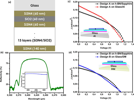
Figure 2: (a) Schematic and (b) reflectivity measurements of dielectric mirror. (c, d) Respective current density−voltage (J−V) curves under AM1.5 illumination of before and after transfer to glass with Al back-reflector and dielectric mirror. Inset: (b) transmittance of polyurethane-based resin.
The researchers were keen to design a structure that could be used in a tandem device that would extract energy from photons of the most suitable energy and transmit lower-energy photons into lower layers. For this they designed a dielectric mirror with ~85% reflectivity in the InGaN QW range, but falling to 20% for longer wavelengths. The dielectrics were applied using plasma-enhanced chemical vapor deposition (PECVD) – 13 bilayers of 60nm silicon nitride (Si3N4) and 60nm silicon dioxide (SiO2), topped off with 140nm silicon nitride.
With the dielectric mirror deposited on glass, followed by transfer, the short-circuit current increased by 12% relative to non-transferred performance. Simulations predicted a 30% increase in current for 85% reflectivity.
The open-circuit voltage was practically unchanged for both transferred set ups.
Hexagonal boron nitride InGaN solar cells InGaN PECVD
https://pubs.acs.org/doi/10.1021/acsphotonics.8b00663
The author Mike Cooke is a freelance technology journalist who has worked in the semiconductor and advanced technology sectors since 1997.


