


- News
24 August 2018
Gallium oxide transistors increase breakdown voltage to 1.8kV
University at Buffalo in the USA claims the highest breakdown voltage measured in a lateral \beta-gallium oxide (Ga2O3) metal-oxide-semiconductor field-effect transistor (MOSFET) to date [Ke Zeng et al, IEEE Electron Device Letters, published online 23 July 2018].
Gallium oxide is a recent material addition to the research effort towards high-power-density devices. Its high critical field enabled the breakdown voltage to be pushed above 1.8kV. Previous work had managed 750V. The improvement is attributed to an improved field-plate design with a composite dielectric supporting the field-plate metal. Atomic layer deposition (ALD) was used for the expected high-field regions of the dielectric, improving material quality.
The device was fabricated using a semi-insulating iron-doped Ga2O3 substrate with two 200nm epitaxial layers of unintentionally doped (UID) and tin-doped (Sn) Ga2O3 (Figure 1). Extra Sn doping was applied selectively to the source/drain regions using a spin-on-glass technique. The metal source/drain contacts were annealed titanium/gold.
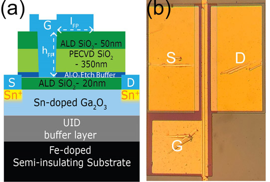
Figure 1: (a) Cross-sectional view and (b) optical image of fabricated field-plated Ga2O3 MOSFET with spin-on-glass source/drain doping.
The gate dielectric consisted of 20nm of ALD silicon dioxide (SiO2). Support for the field-plate structure was provided by plasma-enhanced chemical vapor deposition (PECVD) and more ALD SiO2. The stack also included a thin ALD aluminium oxide (Al2O3) layer designed to serve as a stop for the gate-trench reactive-ion etch. The Al2O3 etch stop was removed from the trench bottom by wet etching. The gate and field-plate metal consisted of titanium/aluminium/nickel/gold. Electrical isolation was provided by a ~220nm-deep reactive-ion etched trench around the device.
Catastrophic three-terminal breakdown (VBR) occurred at 1850V in Fluorinert with a gate-drain distance of 20μm. In an air environment, the breakdown occurred at 440V. Devices with various gate-drain distances demonstrated around 4x the breakdown voltage in Fluoinert, compared with air.
Without Fluorinert, the breakdown is ‘extrinsic’ to the Ga2O3, occurring through air or weaker parasitic paths in the field oxide. The team points out: “Air only has a dielectric strength of 30kV/cm, 266 times lower than Ga2O3 and 333 times lower than SiO2.”
Reducing the gate-drain distance to 1.8μm (Lgd) increased the average electric field in the gate-drain space, calculated as (VBR-Vg)/Lgd, to 2.2MV/cm. Simulations suggest the peak field was around 3.4MV/cm. The critical field of Ga2O3 is predicted to be around 8MV/cm, based on empirical considerations. Other lateral Ga2O3 MOSFETs have achieved 3.8MV/cm, while vertical Schottky barrier diodes have managed 5.1MV/cm.
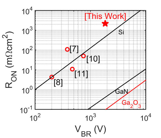
Figure 2: Plot of on-resistance (RON) versus VBR of device under test against previously published lateral Ga2O3 MOSFETs. RON for the Buffalo work calculated at 10V drain bias.
The researchers compared the performance of their work to other reports on lateral Ga2O3 transistors (Figure 2). The overall performance presently seems to hover around the theoretical limit for silicon-based device and falls short of the expected limits for GaN and Ga2O3. The team expects that careful device engineering will be able to push the breakdown higher. The use of Fluorinert could be replaced by more careful passivation.
Gallium oxide transistors MOSFET ALD PECVD
https://doi.org/10.1109/LED.2018.2859049
The author Mike Cooke is a freelance technology journalist who has worked in the semiconductor and advanced technology sectors since 1997.


