


- News
4 April 2018
Zhejiang University develops kilovolt vertical GaN Schottky barrier diode with 825MW/cm2 figure-of-merit
China’s Zhejiang University (ZJU) has developed a 1kV/1.2mΩcm2 vertical GaN-on-GaN Schottky barrier diode (SBD) featuring a high Baliga’s figure-of-merit (BFOM) of 825MW/cm2 and eight-order ON/OFF current ratio at -600V, which is claimed to be one of the best reported for vertical unipolar GaN power rectifiers (‘High-voltage and high-ION/IOFF vertical GaN-on-GaN Schottky barrier diode with nitridation-based termination’ by Shaowen Han, Shu Yang and Kuang Sheng; IEEE Electron Device Letters, vol39, no4, p572, April 2018).
To overcome the challenge of electric field crowding-induced leakage at the junction edge and premature breakdown, the ZJU team has developed a simple planar nitridation-based termination (NT) technique for favorably modifying the GaN surface condition, which can effectively suppress the reverse leakage by over 104 and boost the breakdown voltage up to 1kV.
Furthermore, by using ultraviolet photoemission spectroscopy (UPS) characterization and TCAD (technology computer-aided design) simulations, the researchers have revealed the mechanism of leakage suppression by NT. It is experimentally verified that the NT structure yields an enlarged barrier height and/or effective barrier thickness at the junction edge and, consequently, electron transport via thermionic field emission or tunneling can be suppressed, leading to significantly suppressed edge leakage. This is believed to be the first report revealing the physical mechanism of termination technology that is well suited for high-voltage vertical GaN power devices.
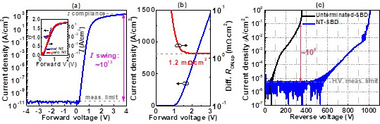
Graphic: (a) Current-voltage (I-V) characteristics of the NT-SBD on a semi-log scale at 25°C. Inset: comparison of I-V characteristics and ideality factor η between the unterminated-SBD and NT-SBD. (b) Forward I-V characteristics of the NT-SBD in linear scale and extracted differential RON,sp of the NT-SBD. (c) Reverse I-V characteristics of the unterminated-SBD and NT-SBD.
Breakdown voltage is boosted from 335V for an unterminated-SBD to 995V after the planar nitridation-based termination. With a differential specific ON-resistance of 1.2mΩcm2, a high ON/OFF current ratio (ION/IOFF at −600V) of ~108 is realized. The 1kV/1.2mΩcm2 vertical GaN SBD exhibits a high current swing of ~1013, large forward current density over kA/cm2, and nearly ideal Schottky contact with a low ideality factor of 1.01‒1.04, showing great potential for high-power and high-frequency applications, says the researchers.
http://ieeexplore.ieee.org/document/8300629


