


- News
16 April 2018
Combining boron nitride and gallium oxide to boost power transistor
Korea University and Korea Electrotechnology Research Institute (KERI) have used hexagonal boron nitride (h-BN) as part of a field-plate structure for β-structure gallium oxide (β-Ga2O3) metal-semiconductor field-effect transistors (MESFETs) [Jinho Bae et al, Appl. Phys. Lett., vol112, p122102, 2018]. The off-state breakdown reached 344V.
Devices based on β-Ga2O3 are being developed in the hope of power electronics applications, based on an ultra-wide 4.85eV direct bandgap and good thermal stability. Theory also suggests that the material has potential for high saturation velocity (~2x107cm/s) and breakdown field (8MV/cm). The Baliga and Johnson figures of merit for β-Ga2O3 are 3214.1 and 2844.4, respectively, which correspondingly compare with gallium nitride’s 846.0 and 1089.0 and with silicon carbide’s 317.1 and 277.8. These figures focus on the suitability of the material for high-frequency power electronics. Another development is larger-diameter commercial β-Ga2O3 substrates beyond the 2 inches of gallium nitride.
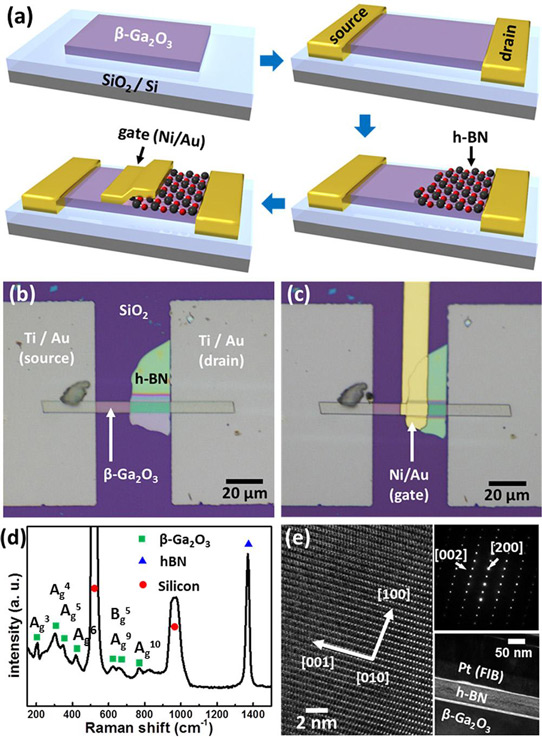
Figure 1: (a) Schematic fabrication process for nano-layer β-Ga2O3 MESFET with h-BN field plate. Optical microscopy images (b) before and (c) after the deposition of top-gate electrode (Ni/Au). (d) Raman spectra of fabricated h-BN/β-Ga2O3 structure. (e) Cross-sectional high-resolution transmission electron microscope TEM image of β-Ga2O3. Insets: selected-area diffraction patterns of β-Ga2O3 flakes (top), and cross section of stacked layers of platinum (Pt) from focused ion-beam (FIB) sample preparation and h-BN/β-Ga2O3 heterostructure (bottom).
The researchers used single-crystal β-Ga2O3 substrate from Tamura Corp for the transistor (Figure 1). The material was mechanically exfoliated into quasi-two-dimensional flakes 200-400nm thick using adhesive tape. The flakes were transferred onto a 300nm silicon dioxide layer on a 500μm-thick silicon substrate. Ohmic source-drain electrodes consisted of annealed titanium/gold. The ~70nm-thick h-BN field-plate insulation material was mechanically exfoliated from bulk powder supplied by Momentive Corp. The transfer to the transistor was assisted using transparent gel-film from Gel-pak to allow for precise positioning. The top gate electrode was nickel/gold.
The h-BN, in addition to having a high dielectric breakdown field of 8MV/cm-12MV/cm, has a high thermal conductivity of 1700-2000W/m-K. The h-BN crystal structure has van der Waals forces linking ‘two-dimensional’ hexagonal layers, allowing thin flakes to be produced by mechanical exfoliation. While β-Ga2O3 is not structured in this way, it does have bond anisotropy that favors cleavage along the (100) face of the crystal lattice. The researchers suggest thinner β-Ga2O3 could be obtained with reactive-ion etch and/or inductively coupled plasma etch.
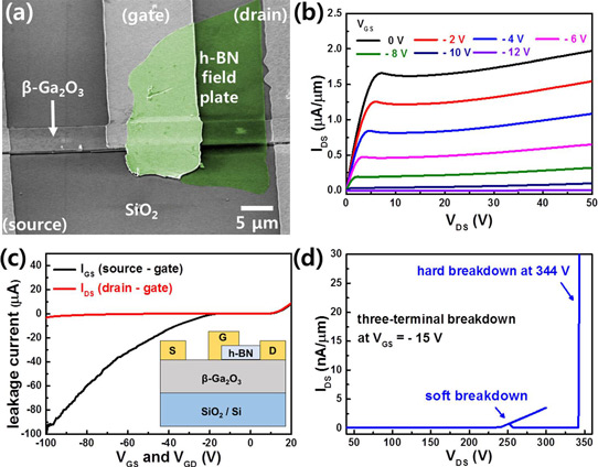
Figure 2: (a) False-color scanning electron microscope image of exfoliated quasi-two-dimensional β-Ga2O3 field-plate MESFET. (b) DC output characteristics of MESFET drain current (IDS) versus bias (VDS) for various gate potentials (VGS). (c) Two-terminal gate leakage current in source-gate and drain-gate regions (inset: schematic of fabricated MESFET). (d) Off-state three-terminal breakdown curve showing soft and hard breakdown voltages.
A gate potential of -12V gave complete pinch-off of the n-channel device (Figure 2). The threshold voltage was at -7.3V. Unlike many common 2D materials such as graphene and transition metal dichalcogenides, these devices had a knee in the current performance with respect to drain voltage, giving a saturation region. The sub-threshold swing was relatively low at 84.6mV/decade, indicating sharp switching behavior. Previously reported β-Ga2O3 transistors have had swings of more than 100mV/decade.
The soft breakdown in pinch-off (gate at -15V) occurred at 250V drain. Complete failure came at 344V. Devices without a field plate broke down at 113V. The researchers suggest that more complex field-plate arrangements could improve the breakdown performance.
Without field plates, the researchers simulated a peak electric field for 200V drain bias of 7.3MV/cm, close to the ~8MV/cm critical field for β-Ga2O3. The simulations used to give the estimate suggest the breakdown occurs near the gate edge. With a field plate, the peak field at 200V was reduced to 4.5MV/cm.
The long-term chemical stability of the device was also investigated, since 2D structures are often vulnerable to degradation from the atmosphere. The researchers stored the device in ambient air for a month. “Device properties including on/off current ratio, saturation current, transconductance, subthreshold swing, and threshold voltage were maintained,” they report.
https://doi.org/10.1063/1.5018238
The author Mike Cooke is a freelance technology journalist who has worked in the semiconductor and advanced technology sectors since 1997.


