


- News
4 April 2018
Improving magnesium doping of aluminium gallium nitride
Y. H. Liang and E. Towe of Carnegie Mellon University in the USA have increased the effectiveness of magnesium (Mg) doping in high-aluminium-content aluminium gallium nitride (AlGaN) material for deep ultraviolet light-emitting diodes (LEDs) produced by molecular beam epitaxy (MBE) [J. Appl. Phys., vol123, p095303, 2018]. Magnesium produces acceptor levels in AlGaN for p-type conductivity through hole transport. Such devices need to bring electrons and holes together so that they can recombine into high-energy photons.
There are a number of factors that restrict the efficiency of most DUV LEDs to a few percent (or less) – among them the poor efficiency of Mg doping in AlGaN. In fact, the efficiency of MBE DUV LEDs is even further restricted to about 0.4%. Last year, metal-organic chemical vapor deposition (MOCVD) was used to give DUVs 275nm LEDs with 20% efficiency [Takano et al, Appl. Phys. Express, vol10, p31002, 2017]. Most DUV LEDs use more established Mg doping of GaN for hole injection, but then many DUV photons are lost through absorption in the narrower bandgap GaN.
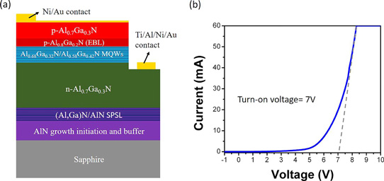
Figure 1: (a) Schematic of deep UV-C LED structure. (b) Current-voltage characteristic.
The epitaxial material was grown on sapphire at ~770°C under liquid-metal-rich conditions – i.e. a monolayer of liquid metal uniformly covered the growth surface. The aim was to produce Al0.7Ga0.3N. In-situ reflection high-energy electron diffraction (RHEED) was used to monitor the process and determine layer thicknesses. The material was fabricated into 500μmx500μm mesa diodes.
Liang and Towe achieved hole carrier concentrations in Al0.7Ga0.3N up to 6x10¹⁷/cm3 with 9.4cm2/V-s mobility. The same techniques used on GaN films achieved up to 5x10¹⁸/cm2 hole density and 5.6cm2/V-s mobility. The activation efficiency of the magnesium (Mg) dopant was 1.2% for Al0.7Ga0.3N. Liang and Towe comment: “This result is intriguing because, in a typical AlN film, only a small fraction (~10-9) of Mg dopants can be activated at room temperature due to the extremely high activation energy, which has been reported to be up to 630meV.”
Temperature-dependent photoluminescence was used to estimate the activation energy of the Mg acceptor levels as 220meV for Al0.7Ga0.3N and 128meV for GaN. Other groups have reported activation energies in the range 408-507meV for Al0.7Ga0.3N, which severely constrains hole carrier concentration.
The metallic monolayer is thought to prevent re-evaporation of dopants at the relatively high substrate growth temperature of 770°C. Also, the high density of Mg atoms may allow ‘banding’ of the acceptor levels, with some levels being closer to the valence band, reducing activation energies.
For n-type doping with silicon, the electron carrier density reached ~1020/cm3 with 130cm2/V-s mobility for GaN and 17.4cm2/V-s for Al0.7Ga0.3N.
The LED material consisted of 30nm AlN nucleation, a 0.2μm AlN buffer, 3nm/3nm (Al,Ga)N/AlN 10-period superlattice strain relief, n-AlGaN cladding, an Al0.58Ga0.42N/Al0.68Ga0.32N 5-period quantum well active region, a 10nm p-Al0.8Ga0.2N electron-blocking layer, and a 150nm Al0.7Ga0.3N contact. The quantum wells were 2nm thick. The barriers were asymmetric – 10nm close to the n-type region and 7nm towards the p-type region. Liang and Towe comment: “The asymmetric design of the quantum-well structure is intended to balance the electron and hole injection levels since these carrier types have different diffusion lengths.”
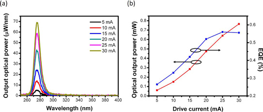
Figure 2: (a) Electroluminescence spectra of output power/nanometer versus wavelength, for deep UV-C LED device with peak emission intensity at 274nm for various drive currents. (b) Optical output power and external quantum efficiency for various drive currents.
The turn-on voltage of the device was ~7V. The near-band-edge emission peak was 274nm with 11nm full-width at half maximum. Output power saturated around 30mA injection to give a value of 0.76mW. This was attributed to the unoptimized structure and thermal effects. The external quantum efficiency and wall-plug efficiency were 0.56% and 0.35%, respectively.
The researchers comment: “Compared to state-of-the-art ultraviolet diodes in the same spectral range, whose film structures are grown by MBE, this generation of devices is an improvement. Even though these device structures were not optimized, we attribute the improvement to the successful achievement of heavy n-type and particularly p-type doping in aluminum-rich (Al,Ga)N films.” They add: “What remains is the design task to optimize the various parameters of the films in the structure now that the fundamental issue for MBE-grown films has been resolved.”
Liang and Towe point out that issues around the directionality of the photon transmission and polarization make light extraction difficult. Also, the impact of defects on radiative recombination needs to be minimized. Liang and Towe see the defects primarily as a substrate problem, which can be solved with the use of (expensive) AlN or AlGaN free-standing substrates.
https://doi.org/10.1063/1.5009937
The author Mike Cooke is a freelance technology journalist who has worked in the semiconductor and advanced technology sectors since 1997.


