


- News
13 September 2017
Thinning p-type III-nitride layers to enhance effects of surface plasmons
National Taiwan University has used a used a magnesium pre-flow during epitaxy to enhance hole concentrations in aluminium gallium nitride (AlGaN) electron-blocking layers in indium gallium nitride (InGaN) light-emitting diodes (LEDs) [Chia-Ying Su et al, Optics Express, vol25, p21526. 2017]. This enabled thinner p-type GaN layers and thus boosted the effect of surface plasmon (SP) structures on LED performance. In particular, a record-high modulation bandwidth of 625.6MHz for c-plane InGaN LEDs is claimed. High modulation bandwidth is desired for visible-light communication application.
Surface plasmons are delocalized electron density oscillations. SP coupling to InGaN quantum wells (QWs) can enhance internal quantum efficiency, while reducing droop effects and increasing bandwidth. Coupling is naturally enhanced as the SPs and QW come into closer proximity. This is achieved by reducing the thickness of the intervening p-type layers from the typical 150nm to the range 38-78nm. Usually the p-GaN layer has to have a certain thickness to ensure adequate current spreading. Thinner p-GaN layers tend to increase turn-on voltage and differential resistance.
The Mg pre-flow also reduces the barrier to injection into the QW active region. The researchers comment: “In this situation, although a decrease of the p-GaN layer may still have the effects of increasing turn-on voltage and differential resistance, the significant enhancement of hole injection efficiency can compensate the performance degradation due to the decrease of p-GaN thickness.”
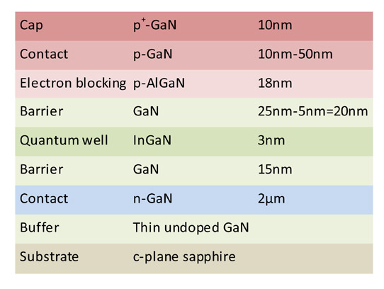
Figure 1: Epitaxial structures of LED.
Epitaxial material for the LEDs came from metal-organic chemical vapor deposition (MOCVD) on c-plane sapphire (Figure 1). The growth of the 18nm p-AlGaN EBL was preceded by a bis(cyclopentadienyl)magnesium (Cp2Mg) pre-flow step at 220 standard cubic centimeters a minute (sccm).
The pre-flow was carried out with the Ga and Al precursors off, but with the ammonia (NH3) nitrogen precursor on. During pre-flow the NH3 decomposed, creating hydrogen that etched back the top GaN barrier by about 5nm, reducing the final thickness to 20nm.
Table 1: Structures and performance of LED samples.
| Sample | A-R | A-SP | B-R | B-SP | C-R | C-SP |
| p-GaN thickness | 50nm | 50nm | 30nm | 30nm | 10nm | 10nm |
| Distance between Ag NPs and QW | — | 108nm | — | 88nm | — | 68nm |
| High-temperature 970°C growth duration | 881s | 881s | 803s | 803s | 726s | 726s |
| IQE | 26.4% | 38.6 | 28.7 | 49.4 | 31.5 | 57.3 |
| SP IQE enhancement factor | — | 1.46 | — | 1.72 | — | 1.82 |
| PL decay time | 2.88ms | 1.35ms | 2.76ms | 1.20ms | 2.63ms | 1.02ms |
| Square-root of SP decay enhancement | — | 1.46 | — | 1.52 | — | 1.61 |
| Normalized output intensity at 3.185kA/cm2 | 1 | 1.67 | 1.19 | 2.06 | 1.30 | 2.48 |
| SP enhancement | — | 1.67 | — | 1.73 | — | 1.91 |
| Droop range at 3.185kA/cm2 | 45.8% | 27.1% | 38.3% | 22.1% | 33.0% | 16.2% |
| SP change | — | −41% | — | −42% | — | −51% |
| Resistance | 44.8Ω | 42.3Ω | 45.6Ω | 43.2Ω | 46.5Ω | 44.3Ω |
| Modulation bandwidth at 9.555kA/cm2 | 349.7MHz | 516.5MHz | 367.2MHz | 559.6MHz | 385.7MHz | 625.6MHz |
| SP enhancement | — | 1.48 | — | 1.52 | — | 1.62 |
For the p-GaN growth the flow of Cp2MG was increased to 280sccm. The 10nm p+-GaN cap used a 800sccm Cp2Mg flow. The substrate temperature during the pre-flow and p-type layers was 970°C.
Reference (R) LEDs were fabricated with 10μm-radius circular mesas. The p-contact pad was not put on the small mesa, but rather supported on a silicon dioxide layer with minimized parasitic capacitance. The p-contact – 20nm/100nm nickel/gold – covered about 80% of the mesa, with the remaining 20% covered with 5nm/5nm nickel/gold for current spreading.
LEDs with surface plasmon structures used 250°C molecular beam epitaxy (MBE) to deposit 10nm gallium-doped zinc oxide (GZO) as a current-spreading layer. The SP structure consisted of silver (Ag) nanoparticles (NPs) and a further current-spreading layer of 5nm/5nm titanium/gold. The p-contact consisted of 20nm/100nm nickel/gold.
The GZO blue-shifts the silver nanoparticle SP resonance wavelength towards that of the blue emissions of the LEDs at ~465nm (Figure 2). The silver nanoparticles were formed by depositing a 2nm silver layer and then annealing at 250°C for 30 minutes in nitrogen atmosphere.
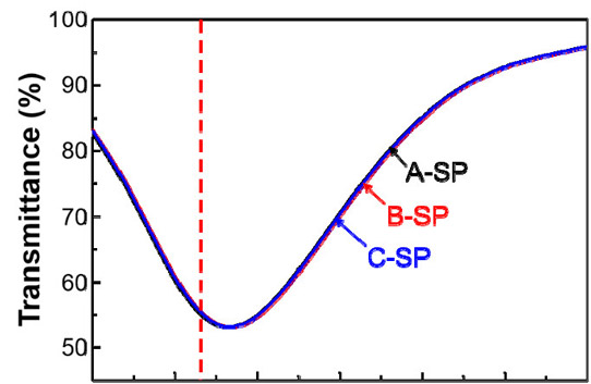
Figure 2: Transmission spectra of samples A-SP, B-SP, and C-SP. Vertical dashed line indicates QW emission wavelength around 465nm.
The researchers comment: “It is noted that the SP resonance peak in the current work does not well coincide with the QW emission wavelength, as shown in [Figure 2]. A careful adjustment of Ag NP size can blue-shift the SP resonance peak for further increasing the SP coupling strength at the designated QW emission wavelength (465 nm). In this situation, the modulation bandwidth can be further increased.”
The n-contacts of the LEDs consisted of 20nm/100nm titanium/gold.
The 970°C growth of the p-type layers also annealed the underlying InGaN single quantum well, reorganizing the indium-rich cluster structures that can lead to higher than expected internal quantum efficiency (IQE) through carrier localization. However, too much annealing can degrade the crystal structure in the quantum well, reducing IQE.
The IQE of the various devices was estimated by comparing the room-temperature photoluminescence (PL) with that at 10K (assumed to be 100% IQE). Shorter anneal times were found to result in higher IQEs (Table 1). The presence of Ag NPs gave significant SP enhancement, particularly with reduced distance to the QW. The decay of time-resolved PL was also faster with SP structures.
The improved IQE of the SP-LEDs resulted in brighter electroluminescence. The droop in wall-plug efficiency (WPE) from the peak value was also less severe in the SP devices. The researchers comment: “It is noted that the injected current density for the maximum efficiencies in the samples under study (1kA/cm2) is generally higher than that usually reported in literature. This is so because the mesa size of the used samples is smaller at 10μm in radius. The smaller device size leads to a weaker heating effect and hence reduces the droop behavior caused by heating.”
The shorter PL decay time is reflected in higher modulation bandwidths, with the highest value higher than 600MHz: “In sample C-SP, we can reach the modulation bandwidth of 625.6MHz, which is believed to be the highest ever reported in a c-plane GaN-based surface-emitting LED (~100MHz higher than our previous record of 528.8MHz).” The improvement over the reference samples is close to the square-root of the enhanced decay rate in the PL studies.
https://doi.org/10.1364/OE.25.021526
The author Mike Cooke is a freelance technology journalist who has worked in the semiconductor and advanced technology sectors since 1997.


