


- News
1 September 2017
Silicon implantation for gallium nitride light-emitting diodes
Southern Taiwan University of Science and Technology and Taiwan’s National Cheng Kung University have used silicon (Si) implantation to create n-type regions on top of indium gallium nitride (InGaN) multiple quantum wells (MQW), allowing a new blue light-emitting diode (LED) structure to be fabricated [Ming-Lun Lee et al, IEEE Transactions on Electron Devices, published online 18 August 2017].
The epitaxial material was grown by vertical metal-organic vapor phase epitaxy on sapphire: 30nm of a GaN 530°C nucleation layer, a 3μm GaN buffer, 2μm of 1000°C n-GaN, 10 well/barrier pairs of 3nm/12nm 750°C In0.2Ga0.8N/GaN, a 100nm 950°C p-GaN cap, and a 2nm n+-GaN tunnel-junction layer.
The silicon ion implant was carried out through a silicon dioxide layer and patterning was supplied by 6μm photoresist (Figure 1). The silicon dioxide scattered the ions to reduce channeling effects where ions penetrate further through the lattice in some directions. After implant, the silicon dioxide and resist were removed using chemical etching. The researchers estimate that the silicon ions penetrated 60nm into the top layer, on average.
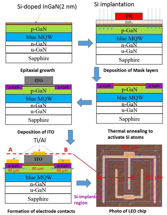
Figure 1: Schematic steps for fabrication of GaN-based MQW LEDs with surface p-n-junction structure formed by selective-area Si implantation into p-GaN top layer.
The n-type doping of the silicon ions was activated with a 90-second rapid thermal anneal at 1000°C in nitrogen. The researchers believe that the n-type doping achieved 3x10¹⁴/cm2 sheet concentration with 21cm2/V-s mobility. The researchers came to these conclusions on the basis of Hall-effect measurements on test wafers without patterning.
The implantation forms a p-n junction above the MQW structure, unlike the usual GaN LED structure where the n-contact is made by etching and making an ohmic contact with the underlying n-GaN layer. The p-contact consisted of a 200nm transparent indium tin oxide (ITO) layer from radio frequency sputtering. The n-contact was electron-beam evaporated titanium/aluminium.
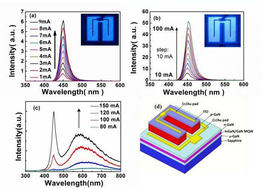
Figure 2: Typical current-dependent electro-luminescence spectra taken from Si-implanted LEDs driven at (a) currents lower than 10mA, (b) currents of 10–100mA, and (c) typical current-dependent spectra taken from conventional LEDs with non-planar p-n homojunction formed by epitaxial growth and subsequent dry etching process, (d) schematic structure of LEDs with nonplanar surface p-n homojunction.
The fabricated LEDs were 300μmx300μm. The electro-luminescence had a single peak at ~450nm (Figure 2). This is unlike the spectrum from conventional GaN LEDs that usually exhibit ‘yellow luminescence’ from defect-related transitions. One might also expect ~365nm near-ultraviolet emission from the p-n junction in the overlying GaN, but this was not seen either. The p-n junction device experienced efficiency droop similar to that seen in conventional mesa LEDs, although beyond 20mA/cm2 there is a slight recovery of EQE.
The researchers think that this may be due to improved carrier diffusion to the MQW at high current. The dynamic resistance is high (greater than 400Ω) but decreases with forward voltage. The rate of descent becomes less steep above 5V (~300Ω), but becomes steeper again above 15V (~150Ω). The 15V mark corresponds to ~20mA/cm2 current. The researchers suggest that the faster decrease in resistance is related to a second current path opening up through the MQW structure. Before 15V the near-surface path dominates, it is suggested.
Si implantation InGaN InGaN MQW Blue LED
https://doi.org/10.1109/TED.2017.2738058
The author Mike Cooke is a freelance technology journalist who has worked in the semiconductor and advanced technology sectors since 1997.


