


- News
6 September 2017
Aluminium nitride nanocolumns on gallium nitride templates
Researchers based in Spain, Germany and France have been studying nanocolumn (NC) selective-area growth (SAG) as a route to high-quality aluminium gallium nitride (AlGaN) materials with high aluminium content [A Bengoechea-Encabo et al, Nanotechnology, vol28, p365704, 2017]. In the reported work, the team from Universidad Politécnica de Madrid in Spain, Otto-von-Guericke University Magdeburg in Germany and CRHEA-CNRS in France grew AlN nanocolumns on GaN templates.
High-Al-content AlGaN is needed for deep ultraviolet (UV) optoelectronics due to the wider bandgaps up to 6.2eV for pure AlN, which corresponds to a wavelength of ~200nm. Presently, AlGaN LEDs emitting wavelengths shorter than 300nm have increasingly miserable efficiency due to high levels of threading dislocations (>108/cm2) and low extraction efficiency of photons due to electromagnetic-wave polarization effects.
High-quality crystalline AlN is expensive and only available in small-area substrates. The researchers hope that nanocolumn growth on GaN-on-sapphire templates could become building blocks for individual nanodevices or the basis for quasi semi-polar or non-polar AlN pseudo-templates due to the high filling factors achieved. Lattice mismatches between high-Al-content AlGaN and the substrate are smaller on AlN, compared with GaN. Growing nanocolumns can reduce strain effects that generate defects. Also, the nanocolumn structuring could improve light extraction.
Other potential applications include micro/nano electromechanical systems using piezoelectric mechanical effects, high-mobility transistors with high breakdown voltage, field-emitters and single-photon emitters.
The AlN nanocolumns were grown by plasma-assisted molecular beam epitaxy (PAMBE) on GaN-on-sapphire templates. Masking for the nanocolumns was provided by a 7nm titanium nitride (TiN) film. The holes in the mask were placed in a triangular net patterned by colloidal lithography. The holes were 170nm diameter with 280nm pitch. The GaN/sapphire template was produced by metal-organic chemical vapor deposition (MOCVD), giving substrates with polar (0001) and semi-polar (11-22) crystal orientations.
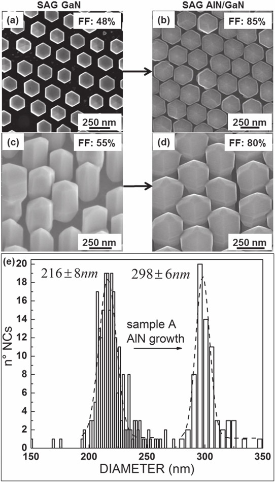
Figure 1: Top-view scanning electron microscope (SEM) pictures of: (a) SAG GaN nanocolumns (NCs) grown on (0001) GaN/sapphire template and (b) after AlN overgrowth (sample A); (c) SAG GaN NCs grown on (11–22) GaN/sapphire template, and (d) after AlN overgrowth (sample B). (e) Diameter distribution before and after sample A’s AlN growth.
The first part of the PAMBE growth was of 860°C GaN nanocolumns to avoid parasitic AlN deposition and nucleation on the TiN mask (Figure 1). The nanocolumn growth was then continued with 860°C AlN deposition. Shadowing effects by the GaN part of the nanocolumn blocked parasitic deposition. The filling factors were higher than 80%.
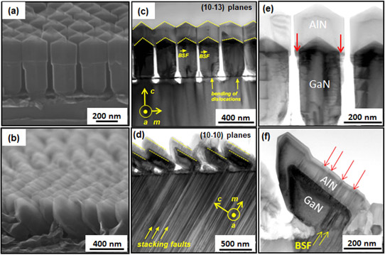
Figure 2: Bird’s-eye view SEM pictures of (a) sample A and (b) sample B. (c) and (d), cross-sectional scanning transmission electron microscope (STEM) bright-field images taken on samples A and B, respectively. Dashed lines mark the main AlN/GaN interfaces and top surfaces. (e) and (f), Cross-sectional STEM bright-field images of individual NCs of samples A and B. Red arrows indicate location of extended defects, found in basal plane.
The nanocolumns on (0001) templates were vertical, while those on (11-22) GaN were inclined 58° from normal with [0001] preferential growth direction. The lengths of the nanocolumns were 450nm in both cases. The diameters of the GaN (0001) and (11-22) structures were 216nm and 221nm, respectively.
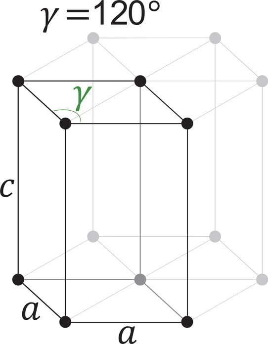
Figure 3: Hexagonal lattice. By Bor75 - Own work, CC BY-SA 3.0, https://commons.wikimedia.org/w/index.php?curid=24101066
The diameter of the (0001) nanocolumns increased to 298nm after AlN growth with a core-shell structure at the interface region. At the same time, the AlN growth in the radial direction seems to be limited so that nanocolumn coalescence does not occur. X-ray analysis resulted in estimates of the AlN ‘c’ and ‘a’ lattice parameters (Figure 3) of 4.982Å and 3.11Å, respectively. The team says that these values are close to being strain-free for AlN. The tops of the columns were pyramidal, consisting of semi-polar {1-103} planes.
The inclination of the (11-22) nanocolumns makes the growth more difficult to describe with uneven exposure to the PAMBE growth (Figure 2). The dominant top surface was the non-polar (1-100) m-plane. The defect density in the non-polar plane was two orders of magnitude lower than in the semi-polar GaN template.
The researchers comment: “The high crystalline quality and the fact that the top facets would reduce or remove the polarization fields in both (Al,Ga)N/GaN and (In,Ga)N/GaN heterostructures make these kinds of nanostructures appealing building blocks, or pseudo-templates, for emitters and detectors working in the deep-UV and UV range whose efficiency nowadays is limited by the quality of the available material.”
Nanocolumn AlGaN AlN nanocolumn GaN templates PAMBE
https://doi.org/10.1088/1361-6528/aa78e6
The author Mike Cooke is a freelance technology journalist who has worked in the semiconductor and advanced technology sectors since 1997.


