


- News
11 October 2017
Indium gallium nitride quantum dot microcavity light emission
Researchers in China have developed tunable indium gallium nitride (InGaN) quantum dot (QD) microcavity (MC) visible light emitters with a 129nm wavelength range from yellow-green to violet from electrical pumping [Yang Mei et al, Appl. Phys. Lett., vol111, p121107, 2017]. The device included distributed Bragg reflectors (DBR) forming the Fabry-Perot cavity.
The team from Xiamen University, East China Normal University, Suzhou Institute of Nano-tech and Nano-bionics (SINANO) and China Academy of Engineering Physics comment: “As the first electrically driven III-V nitride semiconductor based tunable MC light emitter with a tuning range of 129nm, the device is promising for applications such as in wide-gamut compact displays and projectors.”
The researchers also believe that biomedical, mood-lighting, and broad-band communication applications could benefit from monolithic broadband and wavelength tunable light sources.
The semiconductor material (Table 1) was grown on (0001) c-plane sapphire using metal-organic chemical vapor deposition (MOCVD). The QD layer was grown in Stranski-Krastanov mode at 670°C for high indium content. The subsequent GaN barrier was applied in two steps: at 670°C as a 2nm-thick matrix for the QDs to inhibit indium desorption, and then ramped up to 850°C for the 8nm barrier material.
Table 1: Detailed structure of epitaxial wafer.
| Layer structure | Composition | Thickness (nm) |
| Substrate | Flat sapphire | |
| u-GaN | u-GaN | 1000 |
| n-GaN | n-GaN | 4000 |
| Lower cladding layer | n-Al0.1Ga0.9N | 800 |
| Lower waveguide layer | n-In0.03Ga0.97N | 130 |
| Active layers (2 periods) | In0.27Ga0.73N/GaN | 2.5/10 |
| Upper waveguide layer | p-In0.03Ga0.97N | 85 |
| Electron-blocking layer | p-Al0.2Ga0.8N | 25 |
| Upper cladding layer | p-Al0.1Ga0.9N | 600 |
| Contacting layer | p++In0.12Ga0.88N | 20 |
The QD density was ~1.5x10¹⁰/cm2. The indium content was 27%. The dot diameters ranged between 20nm and 60nm. The heights averaged ~2.5nm. Photoluminescence showed a broad spectrum with emissions between 420m and 600nm wavelength. The spread is attributed to variations in dot size and InGaN composition. As the pump power increased there was a blue shift in the spectrum caused by broadening in the small-wavelength region. The researchers attribute this to band filling effects making the bandgap effectively wider.
The electrically pumped MC light emitter (Figure 1) was fabricated first by depositing a 30nm indium tin oxide (ITO) current/spreader layer and ohmic contact on the p-GaN surface of the semiconductor material. The ITO was patterned into a 10μm circular disk to give a narrow current flow path. Silicon dioxide (SiO2) was applied to confine the current aperture to the ITO region. The p-contact electrode consisted of chromium/gold deposited on the SiO2 in a ring that contacted with the ITO. The p-side of the device was completed with 12.5-layer-pairs of tantalum oxide (Ta2O5) and silicon dioxide formed into a 15μm-diameter DBR and 150μm-thick electro-plated copper.
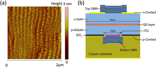
Figure 1: (a) Atomic force microscope 2μmx2μm image of uncapped QDs. (b) Cross-sectional schematic of fabricated InGaN QD MC light emitter.
The n-side was fabricated by removing the sapphire growth wafer through laser lift-off and thinning down to the n-GaN with inductively coupled plasma etch and chemical mechanical polishing (CMP). The n-contact electrode was again chromium gold. The top DBR consisted of 11.5-pairs of Ta2O5/SiO2. The devices were singulated using inductively coupled plasma etch.
Electrical injection without the n-side DBR gave an emission spectrum that was modulated by interference from reflection between the bottom DBR and top GaN/air interface. At low current injection of ~20μA, the emission was dominated by longer wavelengths between 540nm and 570nm. At higher currents the dominant region blue-shifted to 480-520nm. The researchers attribute the changes to the carrier capture and emission properties of the dots with larger QDs dominating at low current and smaller ones at high current. There was a gap in the emissions in the range 530-540nm.
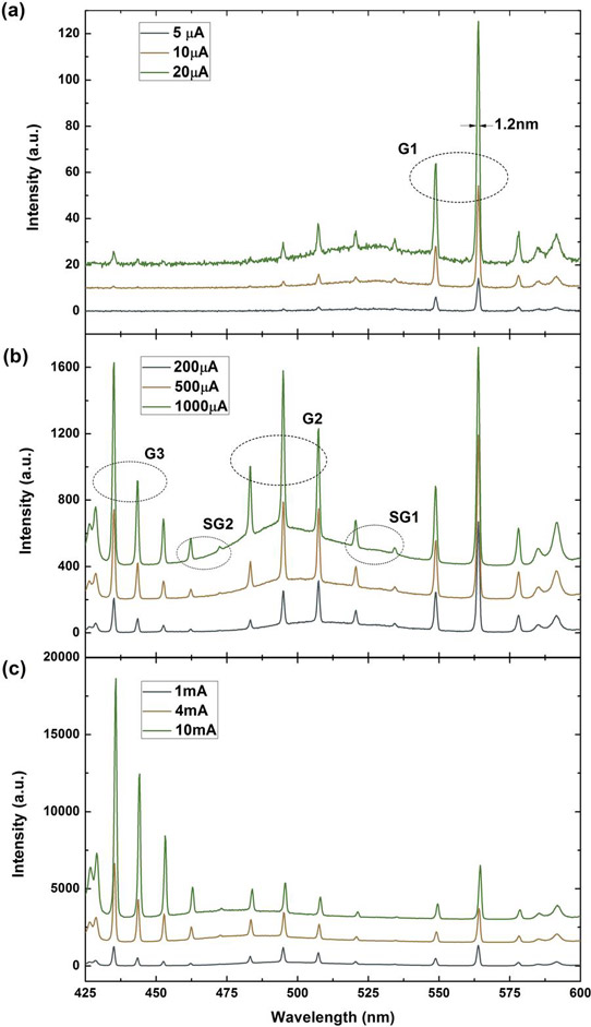
Figure 2: Electroluminescence spectra of MC light emitter at (a) low, (b) medium, and (c) high injected current. All spectra offset along y-axis for clarity.
Cavity effect became more obvious when the second DBR was added. The linewidths were 1.14nm, close to the 1nm limit of the spectrometer. The mode spacings suggested a cavity length of 4.5μm, around 18 wavelengths. The cavity’s quality factor (Q) was around 495. The wavelength composition of the emissions at low current grouped around 560nm (G1, Figure 2). Shorter-wavelength components at ~500nm (G2) and ~440nm (G3) emerge at higher current. The three groups are approximately equal in intensity at around 1mA injection. At 20mA, the emission from G3 was about 7x that from G1.
The 129nm tuning range covered the range from 564nm (yellow-green) to 435nm (violet). The emissions were suppressed around 530nm (SG1) and 470nm (SG2). Simulations suggest that the high emission regions G1-3 correspond to the active QD region being at anti-nodes of the standing waves in the cavity. By contrast, the suppressed groups SG1-2 correspond to the QDs being at nodes of the radiation field.
http://dx.doi.org/10.1063/1.4994945
The author Mike Cooke is a freelance technology journalist who has worked in the semiconductor and advanced technology sectors since 1997.


