


- News
18 October 2017
Thermal curing of SU-8 for bonding gallium arsenide to silicon
University of Virginia and Dominion MicroProbes Inc in the USA have reported the development of submillimeter-wave gallium arsenide (GaAs) quasi-vertical diodes on silicon [Linli Xie et al, IEEE Electron Device Letters, 26 September 2017]. The III-V epitaxial material was transferred to the silicon using SU-8 photoresist as a bonding material. The team worked to eliminate problems with previous methods such as wafer fracture and delamination, which seriously impacted yields.
The researchers comment: “Diodes fabricated with the new process and measured in the 325−500GHz range using on-wafer RF probes exhibit low parasitic capacitance and series resistance, achieving device characteristics comparable to prior state-of-the-art submillimeter-wave diodes.”
The team sees integration of III-V materials on silicon as “an effective approach for realizing novel devices that combine outstanding RF characteristics with a mechanically robust and low-loss substrate”. They add: “Integration processes have been shown to provide flexibility in engineering new device geometries and can be exploited to mitigate the electrical parasitics and thermal grounding bottlenecks that frequently limit the performance of terahertz components.”
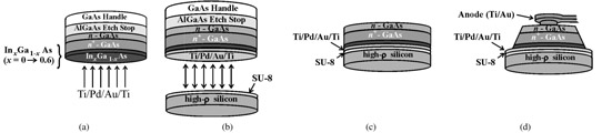
Figure 1: Quasi-vertical Schottky diode fabrication process: (a) Evaporation of Ti (20nm)/Pd (40nm)/Au (150nm)/Ti (20nm) ohmic contact. (b) Bonding of III-V epitaxial material to high-resistivity silicon. (c) Removal of GaAs handle and AlGaAs etch-stop layers. (d) Etching of device mesa and formation of Schottky anode contact.
The researchers have developed a process that builds on previous work (Figure 1). The III-V epitaxial structure on the 650μm-thick GaAs handle wafer consisted of 1μm aluminium gallium arsenide (AlGaAs) etch stop, 280nm n-GaAs, 1μm n+-GaAs device, and highly doped indium gallium arsenide (InGaAs) cap layers. The cap ensured low-resistance ohmic contact with the titanium/palladium/gold/titanium (Ti/Pd/Au/Ti) metal stack. The cap consisted of 50nm graded-composition InGaAs and 40nm In0.6Ga0.4As.
The unannealled metal layers were evaporated over the whole InGaAs surface and were not patterned. By not annealing the metal, a smooth surface was achieved that avoided wafer fracture as a result of the bonding with high-resistivity silicon, which has been a problem with the group’s previous work.
The bonding material was 250nm-thick SU-8 negative epoxy-based photoresist, replacing spin-on glass used previously. “The relatively low curing temperature of SU-8 (100−140°C) compared to SOG (~200°C or higher), coupled with its relatively lower percent volume shrinkage after cross-linking, results in a more robust epitaxy transfer,” the team comments. The low-temperature curing avoided the need for transparent substrates in ultraviolet curing contexts. The bonding involved spin-coating the SU-8, a 1-minute 110°C soft-bake, an ultraviolet exposure, 40 minutes outgasing, and 40 minutes 140°C curing.
The GaAs handle wafer was etched away by 50°C etching in nitric acid and then citric acid solutions. The AlGaAs etch stop was removed by hydrochloric acid.
The diodes were fabricated by etching mesas down to the silicon with a combination of wet and dry etches: sulfuric acid and hydrogen peroxide in deionized water solution wet etch (GaAs); reactive ion etch (Ti, SU-8); sputter etch (Au); and wet chemical etch (Pd, Au). The GaAs mesa was further etched to give semiconductor material on a pedestal of exposed metal.
The further metalization of ohmic and air-bridge finger Schottky contacts, along with other circuit elements, were fabricated using standard techniques.
Direct-current measurements gave 1.19 ideality factor, 4.2Ω resistance, 0.1pA saturation current, 33.7mS/μm2 normalized conductance, and 0.014pA/μm2 normalized saturation current. Reverse-bias breakdown occurred at 9.5V.
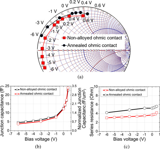
Figure 2: WR-2.2 on-wafer measurement results: (a) S11 versus voltage at 425GHz. (b) Extracted junction capacitance. (c) Extracted series resistance.
High-frequency characterization was carried out for operation in the WR-2.2 rectangular waveguide (0.570mmx0.285mm, 325−500GHz) band (Figure 2). S-parameter characterization focused on the S11 reflection coefficient. The zero-bias junction capacitance normalized to the anode area was 1.78fF/μm2. The normalized series conductance was 38.4mS/μm2. The unannealed ohmic contacts were found to have 1Ω lower series resistance, compared with previous annealed devices.
AlGaAs GaAs Laser diodes Quasi-vertical diodes
https://doi.org/10.1109/LED.2017.2756920
The author Mike Cooke is a freelance technology journalist who has worked in the semiconductor and advanced technology sectors since 1997.


