


- News
6 October 2017
Step-flow growth of green-emitting indium gallium nitride quantum wells
University of Chinese Academy of Sciences has improved green light internal quantum efficiency from indium gallium nitride (InGaN) quantum wells (QWs) by increasing the miscut angle of the gallium nitride template to encourage step-flow growth [Aiqin Tian et al, Appl. Phys. Lett., vol111, p112102, 2017].
The researchers claim that step-flow QWs have not been achieved up to now for green light-emitting InGaN. Instead, green InGaN QWs tend to be formed from two-dimensional (2D) island growth.
The team was partly motivated by the desire for improved green light performance in laser diodes (LDs) for picoprojectors and displays. Indeed, the work included the fabrication of laser diodes with reduced threshold current.
The InGaN QWs were grown on a 2μm n-GaN buffer by low-pressure metal-organic chemical vapor deposition. The QWs consisted of 2.5nm InGaN layers grown at 688°C, while the separating GaN barriers were grown at 850°C.
Ammonia was used for the nitrogen precursor. The gallium component came from trimethyl-gallium for the barriers and buffer and triethyl-gallium for the wells. The indium source was trimethyl-indium.
High-quality step-flow growth for 27%-indium-content green QWs was encouraged by increasing the miscut angle of the GaN/sapphire template from 0.20° to 0.48°. This reduced the step terrace width from ~80n to ~30nm, respectively (Figure 1). This decreased the distance that adatoms had to diffuse on the surface before being incorporated into the step growth front.
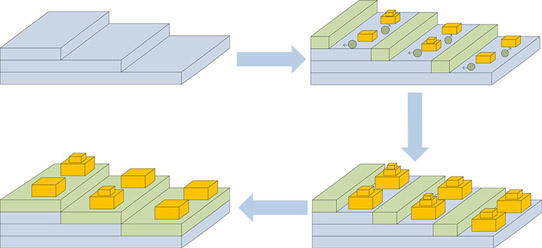
Figure 1: Schematic of 2D island InGaN QW growth on miscut template with large terraces.
The lower growth temperatures needed for high-indium-content InGaN reduces the diffusion distance of adatoms. Blue InGaN QWs with 16% In could be grown at 710°C and 0.20° miscut angle. Higher temperatures increase diffusion distances. Optimized GaN growth occurs at temperatures around 1050°C.
Low-temperature growth with insufficient miscut leads to two-dimensional island or even three-dimensional growth, which can be indicated through increased surface roughness.
Green InGaN 4-period multiple QWs (MQWs) had x-ray diffraction (0002) peak full widths at half maximum (FWHMs) of 351arcsec and 381arcsec for 0.48° and 0.20° miscuts, respectively. The narrower peak suggests sharper well/barrier interfaces from the higher crystal quality achieved through step-flow growth.
Room-temperature photoluminescence (PL) peaks were observed at 2.313eV and 2.309eV for 2D island and step-flow MQWs, respectively. The FWHMs of the peaks were temperature dependent (Figure 2), decreasing to a minimum as the temperature increased to 50K. The room-temperature FWHMs were 131meV for step-flow MQWs and 166meV for 2D island structures.
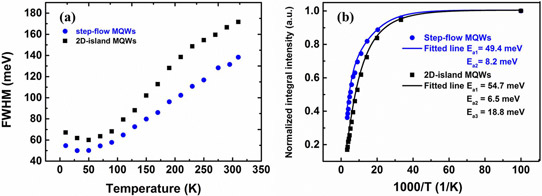
Figure 2: (a) Temperature dependence of FWHM values of green MQW samples. (b) Normalized temperature-dependent integral PL intensity.
The researchers comment: “The smaller FWHM value indicates better potential uniformity, which is beneficial for the improvement of the peak gain of green laser diodes and is believed to result partially from the sharper well/barrier interface, consistent with the XRD result. The indium composition homogeneity may also have improved as a result of the step-flow morphology, but this requires further study.”
Comparing the PL at 10K and room temperature, the internal quantum efficiencies (IQEs) were estimated at 30% and 15% for the step-flow and 2D island samples, respectively. The researchers attribute the IQE improvement for step-flow growth to “better material quality and fewer non-radiative recombination centers in the step-flow MQW sample”.
Temperature-dependent PL analysis suggested also three non-radiative recombination centers in the 2D island sample with activation energies of 54.7meV, 6.5meV and 18.8meV. For the step-flow growth, only two non-radiative recombination centers with 49.4meV and 8.2meV activation were sufficient to fit the data.
The centers with the highest activation energies were attributed to dislocations. The 6.5meV and 8.2meV centers were due to defect formation at the InGaN QW interface, it is suggested. Finally, the 18.8meV center in the 2D island sample is seen as being the factor that significantly reduces IQE.
Laser diodes fabricated from these materials demonstrated the benefit of step-flow growth with reduced threshold current at 300mA, compared with 500mA for the 2D island laser diodes. The researchers attribute this reduction to the improved IQE for step-flow material.
InGaN InGaN QWs Green laser diode
http://dx.doi.org/10.1063/1.5001185
The author Mike Cooke is a freelance technology journalist who has worked in the semiconductor and advanced technology sectors since 1997.


