


- News
22 November 2017
Monolithic indium arsenide quantum dots on silicon optoelectronics
Researchers based in USA, Taiwan and China have monolithically integrated photodetectors (PDs) and lasers using indium arsenide (InAs) quantum dot (QD) in indium gallium arsenide/aluminium gallium arsenide (InGaAs/AlGaAs) well/barrier active structures on silicon [Yating Wan et al, Optics Express, vol25, p27715, 2017]. The devices operated in the 1260-1360nm O-band of wavelengths.
The researchers hope that their work will help to combine the economies of scale of silicon with the high optoelectronic efficiency of III-V materials for photonic integrated circuits . In particular, the InAs QD photodetector showed much reduced dark current compared with germanium-based PDs on silicon.
The team from University of California Santa Barbara (UCSB), Taiwan’s National Central University, Hong Kong University of Science and Technology (HKUST) and Hewlett Packard Labs in the USA report, “to the best of our knowledge, the first characterization of high-speed performance and the first demonstration of the on-chip photodetection for this QD-on-silicon system.”
The researchers see the monolithic integration of photodetectors and lasers on silicon as a means to create power monitors or amplifiers for pre-amplified receivers.
The GaAs-on-silicon template was prepared using metal-organic chemical vapor deposition (MOCVD). The silicon substrate was V-grooved to allow aspect ratio trapping of dislocations. Further cyclic annealing and strain-balancing layers further reduced the dislocation density to 7x10⁷/cm2.
The template was used in molecular beam epitaxy (MBE) to create photodiodes with an active region consisting of seven stacks of InAs dots-in-wells (DWELLs), sandwiched between 1.4μm layers of n- and p-AlGaAs. The epitaxial structure also included 500nm n-GaAs bottom contact layers, and a 300nm GaAs cap. Plan-view transmission electron microscopy of one layer of QDs gave an estimate of 6x10¹⁰ dots/cm2.
Device fabrication (Figure 1) consisted of inductively coupled etching of 20μmx50μm mesas; deposition of palladium/titanium/palladium/gold and palladium/germanium/gold p- and n-contacts, respectively; atomic layer deposition (ALD) of aluminium oxide and sputtering of silicon dioxide passivation; via opening and deposition of 1.5μm titanium/gold ground-signal-ground measurement pads; and, dicing and polishing of photodiode facets without an anti-reflective coating.
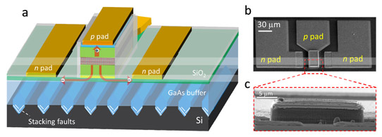
Figure 1: (a) Schematic of fabricated photodetector on V-grooved substrate; (b) top-view and (c) cross-sectional view scanning electron microscope images.
The dark current ranged from 0.8nA to 18nA under reverse biases of -1V and -5V, respectively. Given the 10-5cm2 device area, 1nA corresponds to a current density of 0.1mA/cm2. The researchers point out that 0.08mA/cm2 dark-current density is “two orders of magnitude lower than the competing Ge-on-Si PDs with thin Ge or SiGe buffer layers (typically in the order of 10mA/cm2).” They attribute the improvement to high crystalline quality, low dislocation density, shorter diffusion lengths, and good sidewall passivation.
Coupling a 1.3μm laser source into a photodetector facet with a lensed fiber gave a responsivity of more the 0.3A/W over the 1240-1340nm spectral range. At 1250nm wavelength, the responsivity was 0.33A/W with bias conditions ranging from -1V to -6V. The researchers estimate the facet reflection at around 30% and the coupling loss at 3dB, corresponding to a corrected photodetector responsivity of 0.94A/W. High-quality Ge-on-SOI waveguide photodetectors have been reported with ~1A/W responsivity. “The extracted internal responsivity (0.9A/W) corresponds to 90% internal efficiency,” the team adds.
The frequency performance was measured and model parameters extracted that suggest a (resistance)x(capacitance)-limited 3dB bandwidth of ~2.9GHz. The measured 3dB device bandwidth was slightly lower at 2.3GHz. The researchers attribute the lower value to carrier trapping effects of the QDs.
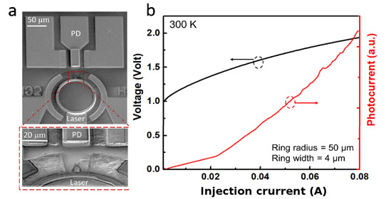
Figure 2: (a) Top-view of fabricated free-space coupled laser-photodetector system; (b) measured laser voltage and detector photocurrent as a function of injection current.
The researchers also integrated the photodetector with a neighboring micro-ring laser (Figure 2). UCSB has been developing lasers on a similar InAs QD platform (www.semiconductor-today.com/news_items/2017/oct/ucsb_131017.shtml). The ring had a 1μmx9μm waveguide to scatter light through free space to the neighboring photodetector. The ring measured 50μm outer radius with 4μm mesa width. The laser threshold was around 21mA, according to the photodetector measurement. A more integrated arrangement (with the laser and photodetector connected by a waveguide) is presently being developed.
Monolithically integrated photodetectors and lasers InAs quantum dot InGaAs AlGaAs MBE
https://doi.org/10.1364/OE.25.027715
The author Mike Cooke is a freelance technology journalist who has worked in the semiconductor and advanced technology sectors since 1997.


