


- News
29 November 2017
Ex-situ aluminium nitride on silicon templates for light-emitting diodes
South China University of Technology has been studying the use of ex-situ low-temperature pulsed laser deposition (LT-PLD) to create aluminium nitride on silicon (AlN/Si) templates for indium gallium nitride (InGaN) light-emitting diodes (LEDs) [Haiyan Wang et al, IEEE Transactions on Electron Devices, vol64, p4540, 2017]. The researchers began their work with ultra-high-vacuum PLD of aluminium nitride on cleaned silicon (111) substrates at 650°C. The template growth was carried out in nitrogen plasma generated by radio-frequency excitation. The aluminium came from sintered AlN, which was ablated by 200mJ krypton fluoride excimer laser pulses repeated at 30Hz.
The hope is that such work will reduce manufacturing costs from the use of much less expensive substrates, compared with gallium nitride, silicon carbide, or sapphire. The team produced 0.5mmx0.5mm LEDs with light output power of 70.2mW at 300mA current injection.
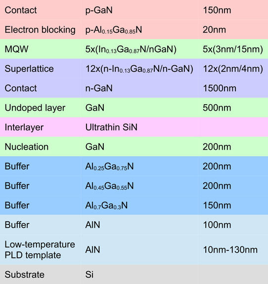
Figure 1: LED epitaxial structure.
The LED material was grown on the low-temperature AlN/Si templates by metal-organic chemical vapor deposition (Figure 1). The structure includes a number of layers to bridge the mismatches between GaN and Si in terms of lattice parameters (16.9%) and thermal expansion (54%) that can reduce crystal quality and induce cracking of the material on cooling. The templates had a varying thickness of low-temperature AlN, ranging from 10nm to 130nm. The materials were fabricated into standard lateral 500µmx500µm LEDs.
X-ray analysis suggested that a 40nm AlN/Si template gives the best crystal quality in subsequent metal-organic chemical vapor deposition (MOCVD). The team explained the quality trend as being due to the smoother surface morphology of the 40nm sample, which also has a large number of small AlN grains that can act as nucleation sites for subsequent lateral growth. By contrast, thicker AlN templates have large islands of AlN that coalesce and present a rough surface, potentially reducing surface mobility of precursors and retarding AlN buffer coalescence. Also, the 40nm (and 70nm) AlN/Si template resulted in crack-free material. Larger AlN thickness templates tended to result in cracked heterostructures.
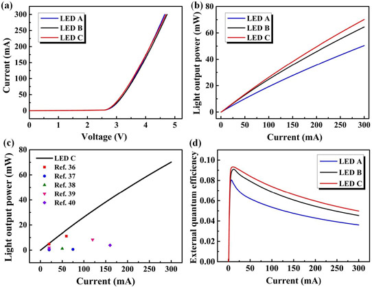
Figure 2: (a) Current versus voltage, (b) light output power versus current for LEDs A, B and C, (c) comparison of light output power of LED C with previously reported values, and (d) EQE versus current for LEDs A, B and C.
In terms of light output power, LEDs based on 70nm AlN/Si templates (LED-C) gave the highest value of 70.2mW at 300mA injection current (Figure 2). This compares with 50.4mW for LED-A on a 10nm AlN/Si template. The power from LED-C was also 9% greater than that from LED-B on 40nm AlN/Si. The power output was also greater than previous reports, corrected for device size, as shown in Figure 2(c). The peak external quantum efficiency (EQE) of LED-C was 9.3%. At 300mA, the EQE fell to around 5%. The efficiency droops between the peak and 300mA for LEDs A-C were 55.1%, 50.1%, and 46.2%, respectively.
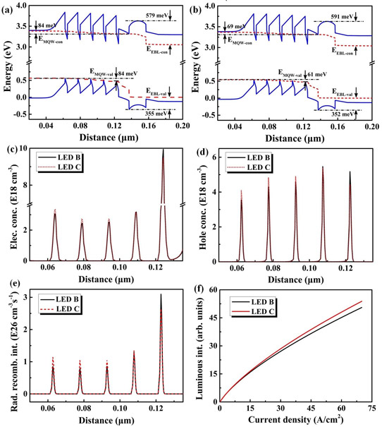
Figure 3: Band diagrams of (a) LED B and (b) LED C at a current density of 35A/cm2. The blue solid line and red dashed line represent the energy band and Fermi energy, respectively. (c) Electron concentration, (d) hole concentration, (e) radiative recombination intensity, and (f) simulated luminous intensity of LEDs B and C, respectively.
Since the light was strongly absorbed by the underlying silicon, higher output would result from substrate removal and the use of thin-film flip-chip LED chip manufacturing processes. Simulations of the structures suggested that LED-C benefited from higher and more uniform carrier concentrations across the quantum wells, boosting output power (Figure 3).
AlN on silicon templates AlN LEDs InGaN MOCVD
https://doi.org/10.1109/TED.2017.2753844
The author Mike Cooke is a freelance technology journalist who has worked in the semiconductor and advanced technology sectors since 1997.


