


- News
8 November 2017
Reverse-blocking gallium nitride on silicon high-electron-mobility transistor
École polytechnique fédérale de Lausanne (EPFL) in Switzerland has claimed a record high reverse breakdown voltage (VRB) of 900V for a reverse-blocking gallium nitride on silicon (GaN-on-Si) metal-oxide-semiconductor high-electron-mobility transistor (MOSHEMT) [Jun Ma et al, IEEE Electron Device Letters, 11 October 2017]. The reverse blocking was enabled by an integrated tri-anode Schottky drain structure with metal wrapped around etched nanowires.
The forward-bias breakdown (VFB) was also high at 800V and 20nA/mm with grounded substrate. The team comments: “Both the high VFB and VRB were achieved in a single integrated device in this work, instead of using a discrete transistor in series with an SBD [Schottky barrier diode], which can greatly simplify the circuit design, reducing its size, resistance and parasitic components, and improve the efficiency of power converters.”
In particular, reverse-blocking transistors are needed for cyclo-converter, matrix converter, current source and multi-level inverter circuit formats. Up to now, integrated reverse-blocking devices have tended to have low reverse breakdown (less than 685V) and/or high reverse current leakage (more than 0.4μA/mm). By contrast, EPFL’s single integrated device has performance comparable to circuits using state-of-the-art discrete devices.
The epitaxial structure (Figure 1) consisted of a 2nm GaN cap, 24nm aluminium gallium nitride (Al0.25Ga0.75N) barrier, 300nm GaN channel, and 5μm buffer. The two-dimensional electron gas near the barrier/channel interface had a measured carrier concentration of around 1x10¹³/cm2 with 2000cm2/V-s mobility.
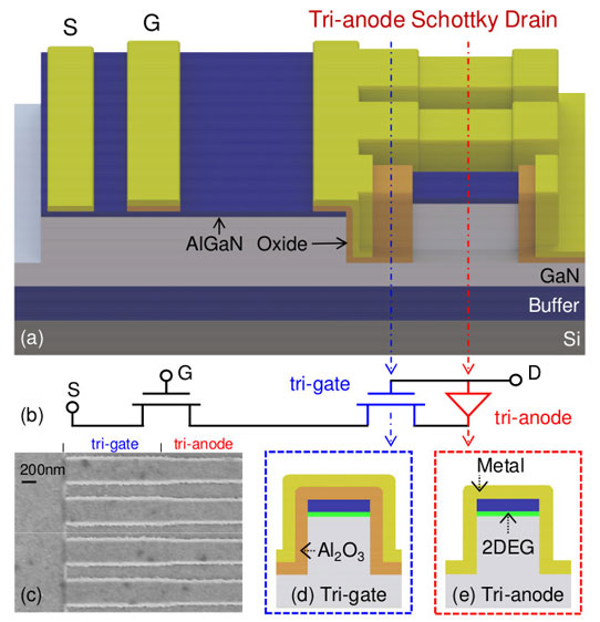
Figure 1: (a) Schematic and (b) equivalent circuit of reverse-blocking MOSHEMT. (c) Top-view scanning electron microscope image of hybrid tri-anode Schottky drain and schematic cross-sections of (d) tri-gate and (e) tri-anode regions.
The nanowires for the drain region were etched to a depth of 180nm by inductively coupled plasma. The width and spacing of the wires were 300nm, giving a 50% fill factor. The devices were electrically isolated through mesa etching. The ohmic source contact consisted of titanium/aluminium/titanium/nickel/gold, annealed at 830°C in forming gas (hydrogen and nitrogen) for 30 seconds.
The oxide insulation layers – 10nm silicon dioxide and 10nm aluminium oxide – were applied by atomic layer deposition (ALD). Selective removal of the oxides was performed in the tri-anode region to give a Schottky contact. The gate and drain contacts were nickel/gold. Wet etching removed the oxide materials in the access and ohmic contact region. The lack of passivation from oxides in these regions did not affect leakage, according to the researchers.
The physical dimensions of the device were 1.5μm gate-source, 2.5μm gate length, 12.5μm gate-drain. The field plate (FP) was 1.3μm; the tri-gate region 1.2μm. The device width was 60μm. The team comments: “The tri-gate region (Figure 1(d)) works as tri-gated FPs to shield the tri-anode region from high voltages, which along with the planar FP improves the VRB.”
The RB-MOSHEMTs had a maximum drain current of 520mA/mm and a differential on-resistance of 14Ω-mm, normalized to the width of the device. A reference device with ohmic drain achieved a higher current (550mA/mm) and lower resistance (13Ω-mm). The researchers suggest that the difference could be made up by increasing the fill factor of the tri-anode region. The turn-on voltage for the RB-MOSHEMT was 0.58V. The forward drain bias for 150mA/mm current was 2.1V in the reference transistors and 2.9V for the RB-MOSHEMT.
The (non-blocking) reference had a 280mA/mm current when the drain was reverse biased at -15V. At the same voltage, the RB-MOSHEMT had a leakage current 19nA/mm, a factor of 7 orders of magnitude difference. The blocking was independent of the gate potential over the range from -10V to +5V.
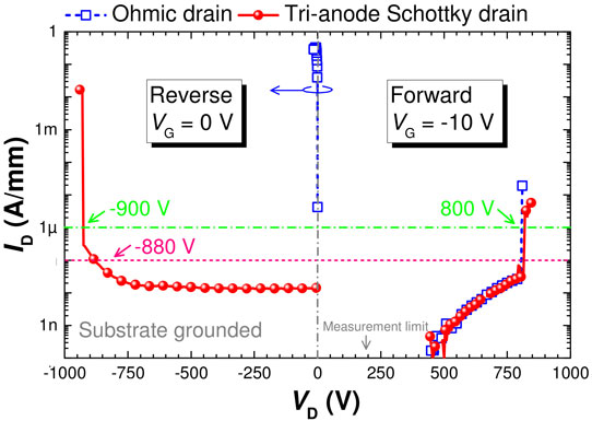
Figure 2: Breakdown characteristics of RB-MOSHEMTs and MOSHEMTs measured at room temperature with grounded substrate.
The gate threshold for 1μA/mm was -6.6V for both devices. The subthreshold swing and on/off current ratios were also similar, at 100mV/decade and 1010, respectively. The subthreshold swing suggests an oxide/semiconductor interface trap density of 1.24x10¹²/cm2-eV,
At 150°C, the on-voltage decreased to 0.53V, while the on-resistance increased to 26Ω-mm. The reverse blocking current also increased by an order of magnitude to 0.57μA/mm (570nA/mm). This is still below 1μA/mm, indicating “excellent potential of the RB-MOSHEMTs for high-temperature applications,” the researchers say.
The forward breakdown of the devices occurred at 800V with the gate potential at -10V and 0.02μA/mm current. The off-current at 650V was 6nA/mm. The reverse blocking of RB-MOSHEMTs broke down at around -900V. The current at -750V was 0.02μA/mm.
The team comments: “The high VRB obtained in this work is attributed to the better-distributed electric field under reverse biases. In the hybrid tri-anode drain, two field plates (e.g. the planar and the tri-gate regions) are integrated with the tri-anode, by simply engineering their pinch-off voltages with the tri-gate approach, which spread effectively the electric field and improved the VRB.”
https://doi.org/10.1109/LED.2017.2761911
The author Mike Cooke is a freelance technology journalist who has worked in the semiconductor and advanced technology sectors since 1997.


