


- News
26 May 2017
Optimizing trench profiles for power gallium nitride electronic devices
Researchers in the USA and Singapore have been seeking to optimize electric fields in trench-based gallium nitride (GaN) power electronic devices with vertical architectures [Yuhao Zhang et al, Appl. Phys. Lett., vol110, p193506, 2017].
The vertical structure should push peak fields deep inside the GaN material, avoiding premature breakdown through surface effects. A number of groups have reported trench-based devices including Schottky rectifiers, fin field-effect transistors (FETs), metal-oxide-semiconductor field-effect transistors (MOSFETs), and current-aperture vertical electron transistors.
The team from Massachusetts Institute of Technology (MIT) in the USA, Singapore-MIT Alliance for Research and Technology, and IQE RF LLC in the USA comments: “Among the demonstrated vertical GaN power devices, trench-based structures have achieved the best performance for advanced Schottky rectifiers and power transistors.”
However, electric (E) fields crowd around sharp corners, leading to premature breakdown. The dry etch techniques used to create trenches tend to result in such sharp corners and rough sidewalls that encourage unwanted current leakage. Although heating the structure can round off trenches and smooth sidewalls, such annealing degrades material quality. Another approach is a second etch using wet solutions, which is slower but can also smooth rough sidewalls.
The researchers etched wafers with n--GaN layers on 2-inch silicon or n+-GaN substrates. The trench process was developed using samples on silicon, while trench-based devices were produced on free-standing GaN.
The dry etch part consisted of boron trichloride (BCl3) and chlorine (Cl2) inductively couple plasma processing through nickel hard masks, giving trenches of the order 2μm wide and deep. “Compared with conventional oxide masks, the use of a metal hard mask allows for a much smoother etch sidewall, due to the lack of oxide edge erosion under high ion energies,” the team writes.
Corner rounding and etch-damage repair was achieved using tetramethylammonium hydroxide (TMAH) wet etching and piranha clean. The 70-minute 85°C TMAH etch was anisotropic, preferring to eat the sidewalls. The researchers found only slight differences in smoothness (~20nm) for trenches aligned to different crystal orientations subjected to TMAH treatment. The 10-minute piranha clean removed nickel mask residues.
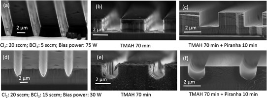
Figure 1: Cross-sectional scanning electron micrographs of trench structures right after dry etching, with following TMAH wet etching, and additional piranha clean, for two different conditions of initial dry etching.
The dry etch could also be adjusted to provide either flat-bottom or tapered-angled-bottom trenches (Figure 1). The researchers explain: “A less anisotropic dry etching could enhance the lateral etching, reduce the tapered angle of dry etching sidewalls, and produce a tapered trench bottom after the TMAH wet etching. In the Cl2/BCl3 based ICP etching, the less anisotropic etching can be realized by either reducing the bias power or increasing the BCl3/Cl2 ratio.”
Dry etch with lower bias power and higher BCl3 flow rate produced a pointed trench bottom that became rounded after wet etch treatment.
Trench metal-insulator-semiconductor barrier Schottky (TMBS) rectifiers were produced with various trench profiles: unrounded, rounded with tapered bottom, and rounded with flat bottom (Figure 1). After etching, the structure was coated with 250nm of plasma-enhance chemical vapor deposition (PECVD) silicon nitride. The top Schottky contacts consisted of nickel/gold. The backside contact was titanium/aluminium, giving an ohmic contact.
Without rounded trench corners, the device suffered from reverse-bias leakage and breakdown at only -150V (Figure 2). The researchers attribute the leakage mainly to trap-assisted space charge limited current: “The dominant traps are probably located at the etching sidewalls and their interfaces with dielectrics.”
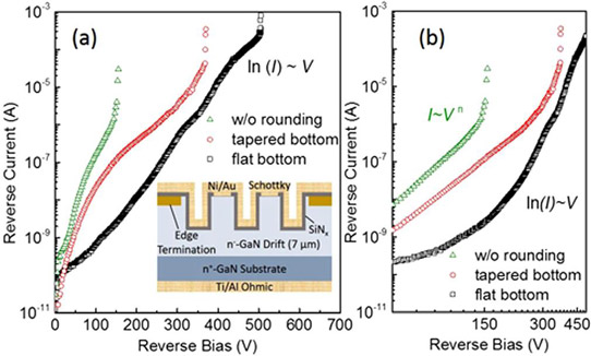
Figure 2: (a) Reverse I-V characteristics of TMBS rectifiers with non-rounded trenches, rounded flat-bottom trenches and rounded tapered-bottom trenches, in semi-log plot. Inset: schematic structure of fabricated GaN TMBS rectifiers. (b) Reverse I-V characteristics in log-log plot.
The structure with flat-bottom rounded-corner trenches gave the lowest reverse-bias leakage current and highest breakdown at-500V. The leakage is attributed mainly to variable-range-hopping through dislocations. The team comments; “This indicates that, in the TMBS rectifiers with rounded flat-bottom trenches, the leakage current is mostly determined by the peak E-field in bulk GaN rather than dielectrics or dielectrics/GaN interfaces.”
The rounded tapered-bottom rectifiers came between the leakage and breakdown (-350V) performance of the previous two devices. The leakage is attributed mainly to a combination of the dominant factors affecting the unrounded and the flat-bottom devices.
The researchers foresee that, by using the optimized trench, further current-blocking improvement could come from “enhancement of dielectric quality, insertion of implanted field rings near the trench bottoms, or introduction of carbon-doped GaN/p-GaN hybrid blocking layers.”
Tetramethylammonium hydroxide wet etch GaN Schottky rectifiers FETs MOSFETs
http://dx.doi.org/10.1063/1.4983558
The author Mike Cooke is a freelance technology journalist who has worked in the semiconductor and advanced technology sectors since 1997.


