


- News
19 May 2017
Indium gallium nitride light-emitting diodes on thin industry-spec silicon
Researchers in Singapore and USA have been developing ways to grow III-nitride structures on SEMI-spec 200mm-diameter silicon by metal-organic chemical vapor deposition (MOCVD) [Li Zhang et al. Semicond. Sci. Technol., vol32, p065001, 2017].
Ordinarily such structures are grown on relatively thick silicon wafers (1mm-1.5mm) to avoid breakage in wafer handling caused by hidden stress in indium aluminium gallium nitride (InAlGaN) layers from lattice mismatch and high-temperature growth and cooling processes. Unfortunately, 200mm silicon wafer manufacturing facilities are based on tools designed to meet specifications of the Semiconductor Equipment and Materials International (SEMI) industry organization, which specifies 725μm (0.725mm) thicknesses or thinner.
The Singapore-MIT Alliance for Research and Technology, the National University of Singapore, and Massachusetts Institute of Technology (MIT) see the work as part of their efforts towards “integration of GaN and Si CMOS as the driver for GaN-on-Si materials and device development”. GaN materials are being used and developed for both high-power, high-voltage and high-frequency electronics, along with the longer-term light-emitting (LED) and laser diode applications.
The team used MOCVD equipment with a specially shaped pocket susceptor. A flat susceptor suffers from uneven heating of the substrate. With concave bowing caused by stress, the contact is made in the center of the wafer, giving higher temperatures there. With convex bowing, the temperature is higher toward the edge. The researchers designed a concave pocket with 12 400μm-high protusions placed radially at 30° separation so that the substrate was suspended above the susceptor, giving more even heating. Bowing of the wafer, if excessive, can cause plastic deformation of the substrate, increasing fragility.
The researchers explain: “By suspending the wafer with 12 protrusions, this design ensures that during the entire growth run, the wafer is not in contact with the susceptor except at the protrusions. As a result, maintaining a uniform temperature across a SEMI-spec 200mm-diameter silicon wafer can be more easily achieved during the entire growth process.”
After native oxide removal and pre-treatment of the 200mm-diameter SEMI-spec boron-doped silicon wafer, MOCVD began with 20nm low-temperature (980°C) AlN nucleation.
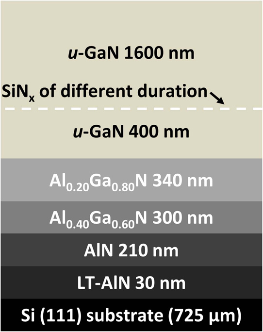
Figure 1: Schematic of optimized epitaxial structure of GaN-on-Si growth for LEDs.
The temperature was then ramped for 240nm high-temperature AlN, followed by step-graded layers of AlGaN to bridge over to the final GaN layer (Figure 1). The AlGaN layers also introduce compressive strain that was designed to compensate for tensile strain that usually develops when GaN-on-silicon structures are cooled to room temperature.
The AlN initial part of the growth, from tensile strain due to lattice mismatch with silicon, gives a concave wafer bow. The AlN to GaN step-grading converts this to convex bowing. The final cooling results in an approximately flat wafer due to differences in the coefficients of thermal expansion of the various layers.
LED material was grown on 0.4μm undoped GaN template on silicon with layer sequence: 2.4μm n-GaN, 3x 1.5nm InGaN/40nm GaN V-pit initiation, 10x-15x 2.5nm InGaN/10nm GaN multiple quantum wells/barriers (MQWs), p-AlGaN electron blocking, and p-GaN and p++-GaN for ohmic contact.
V-pits roughen the surface (Figure 2) and give three LED performance advantages. According to the researchers: “The thinner MQWs on the sidewall enhance the efficiency of LEDs in several ways: (i) form a potential barrier to non-radiative recombination; (ii) improve hole injection into the MQWs; (iii) reduce reverse leakage current in the LEDs.”
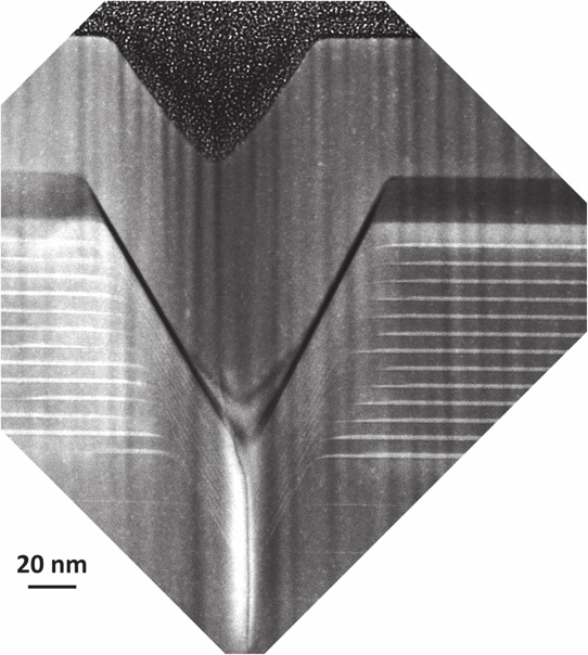
Figure 2: Cross-sectional scanning transmission electron micrograph of V-pit initiation layers and MQWs.
Since the V-pits tend to nucleate on threading dislocations (TDs), the density of V-pits gives an indication of TD density (TDD). For the optimized 450nm-wavelength LED structures the V-pit density was 5.5x10⁸/cm2. This compares with a minimum V-pit density of 2.7x10⁸/cm2 for LEDs produced on thicker (1mm) non-SEMI silicon.
The LEDs on SEMI-spec silicon had an internal quantum efficiency of about 70%. For 300μmx300μm devices, the typical turn-on voltage was 2.5V. Reversed bias leakage was 0.2nA at -4V. Diode ideality was 2.3.
Before producing the LEDs, the researchers worked to optimize the growth processes, in particular step-graded AlGaN structure. A three-step AlGaN layer sequence – 280nm Al0.8Ga0.2N, 300nm Al0.4Ga0.6N, 310nm Al0.2Ga0.8N – resulted in minimum concave bow of -4μm. However, the generation of edge-type threading dislocations (TDs), as indicated by x-ray analysis, increases with decreasing Al0.2Ga0.8N layer thickness.
“Generally, edge-type dislocations are more detrimental to device performance and reliability, causing reliability issues in HEMTs [high-electron-mobility transistors] and increasing non-radiative recombination in the MQWs of LEDs,” the team comments. Increasing the Al0.2Ga0.8N layer to 395nm reduced the (102) x-ray peak to 670 arcsec, from 750 arcsec for the minimum bow 310nm layer. However, the wafer bow increased to +72μm convex.
The researchers used a silicon nitride (SiNx) masking layer in the middle of the u-GaN growth as a technique to balance low bowing with low TDDs. In particular applying silicon nitride on GaN can create a SiGaN3 monolayer that acts as an anti-surfactant, inhibiting GaN growth. The team comments: “We use the anti-surfactant behavior of SiNx masking to moderate the strain of the subsequently grown GaN layer from the masked GaN layer.”
Further GaN growth is from uncovered regions, which reduces dislocation densities. The growth from the uncovered island regions coalesces to form laterally overgrown GaN material. The amount of coverage by SiGaN3 was controlled by the duration of exposure to disilane (Si2H6) and ammonia (NH3) precursors.
The researchers produced an optimized GaN template for LEDs with a 2-step AlGaN buffer combined with 150-second SiNx masking that was used for the LED material. A 2-step buffer was found to increase the compensating compressive stress within a thinner layer to counteract bowing.
InGaN LEDs InGaN LEDs 200mm-diameter silicon MOCVD
https://doi.org/10.1088/1361-6641/aa681c
The author Mike Cooke is a freelance technology journalist who has worked in the semiconductor and advanced technology sectors since 1997.


