


- News
17 May 2017
Indium gallium arsenide quantum well transistors on 300mm silicon
Researchers in South Korea and the USA claim record 2190cm2/V-s effective mobility for indium gallium arsenide (InGaAs) quantum well (QW) metal-oxide-semiconductor field-effect transistors (MOSFETs) on 300mm-diameter (100) silicon substrates [Seung-Woo Son et al, IEEE Electron Device Letters, published online 19 April 2017].
InGaAs MOSFETs are being developed for the n-channel part of next-generation low-power logic complementary MOS circuits. InGaAs benefits from higher electron mobility and injection velocity compared with silicon. This should allow a reduction of operation voltages to below 0.5V, reducing power dissipation.
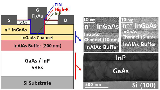
Figure 1: (a) Schematic of InGaAs QW-MOSFET, and (b) cross-sectional transmission electron micrographs with channel thicknesses of 10nm and 5nm.
Kyungpook National University and Samsung Electronics of South Korea, University of Texas at Austin in the USA and Ulsan University in South Korea grew their semiconductor material by metal-organic chemical vapor deposition (MOCVD). The transistor structure (Figure 1) used GaAs and indium phosphide (InP) layers to create a strain relaxation buffer (SRB) on the silicon wafer. This was followed by indium aluminium arsenide (In0.52Al0.48As) buffer and an ultra-thin-body In0.53Ga0.47As channel. The device layers were completed with an InP etch stop and In0.53Ga0.47As cap.
The MOSFETs were fabricated with mesa isolation, molybdenum/titanium/platinum/gold ohmic source-drain electrodes, plasma-enhanced chemical vapor deposition (PECVD) silicon dioxide passivation, aluminium oxide/hafnium dioxide gate dielectric, atomic layer deposition (ALD) titanium nitride gate metal, and titanium/gold gate contact.
With a 5nm channel thickness and 3μm gate length, the transistor achieved 50μA/μm maximum drain current and 6000Ω-μm on-resistance. With drain bias at 0.5V, the maximum transconductance was 100μS/μm. The subthreshold swing was 75mV/decade, while the drain-induced barrier lowering (DIBL) was 8mV/V.
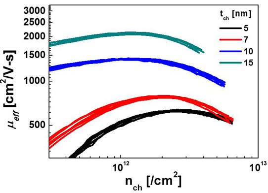
Figure 2: Effective mobility (μeff) plotted against channel carrier concentration (nch) for InGaAs MOSFETs on Si from 10μm to 4μm, with different values of channel thickness (tch).
The researchers studied devices with varying channel thickness (15nm-5nm), finding that thinner channels reduced drive current and transconductance performance, as expected. The thinner channels also suffered from reduced effective mobility (Figure 2). The researchers attribute this to increased surface roughness and Coulomb scattering in the thin channel devices.
The root-mean-square roughness was assessed at close to 1nm, according to atomic force microscopy (AFM). This is rougher than what has been achieved in InGaAs/InAlAs QW MOSFETs on InP substrates. Coulomb scattering is associated with interface states that trap charges.
The team suggests that process optimization should aim at “defect-free growth of InGaAs/InAlAs QW MOSFETs on Si with smooth surface morphology”.
With a 15nm channel thickness, the researchers achieved what they consider to be the best combination of high effective mobility (2140cm2/V-s) and low subthreshold swing (90mV/decade), beating the results of other groups’s InGaAs QW MOSFETs in both respects.
InGaAs Quantum well MOSFET MOSFETs Silicon substrates MOCVD
https://doi.org/10.1109/LED.2017.2695652
The author Mike Cooke is a freelance technology journalist who has worked in the semiconductor and advanced technology sectors since 1997.


