


- News
3 May 2017
Epitaxial lift-off and wafer bonding for III-V photodetectors on silicon
Researchers in Korea have been developing low-production-cost epitaxial lift off (ELO) techniques for wafer-bonded III-V photodetector (PD) transfer to silicon (Si) [SangHyeon Kim et al, Appl. Phys. Lett., vol110, p153505, 2017]. The devices were based on ‘pin’ (p-type/intrinsic/n-type) absorbing structures, but the researchers from Korea Institute of Science and Technology, University of Science and Technology (UST) and Seoul National University believe that the method is extendable to typical gallium arsenide photodetector structures such as quantum well infrared photodetectors and quantum dot infrared photodetectors.
GaAs-based PDs benefit from the better carrier photogeneration response to photons, resulting from having a direct bandgap (unlike Si, which has an indirect bandgap). However, GaAs is a more expensive material. Wafer-bonding on silicon and reuse of the III-V growth substrate could be a route to reducing costs. Also, hybrid integration could allow III-V PDs to be integrated to versatile silicon electronics readout and data processing capabilities.
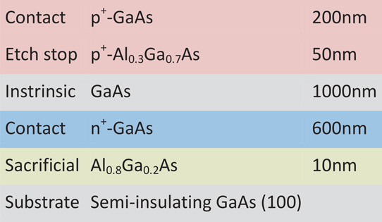
Figure 1: Layer growth of pin diode structure.
The ELO works by dividing up the material to be transferred to silicon into mesas, allowing the etchant used to release the III-V growth substrate by more speedy access to an aluminium gallium arsenide (AlGaAs) sacrificial layer. The pin diodes were grown on 1.5cmx1.5cm semi-insulating GaAs (100) substrate by molecular beam epitaxy (MBE) – see Figure 1.
The ELO process (Figure 2) began with depositing palladium/gold on both the pin diode material and the target silicon substrate. The metal stack acted both as bonding for the III-V/silicon structure and as a bottom electrode for the p+GaAs contact of the PDs.
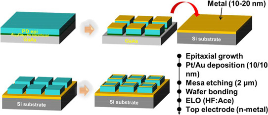
Figure 2: Fabrication scheme for GaAs pin PD on Si using wafer bonding and ELO.
Before bonding, the III-V wafer was patterned and etched with phosphoric acid (H3PO4) solution down to the sacrificial AlGaAs layer.
The ELO process continued with argon plasma activation of the metal surfaces for wafer bonding at room temperature with uniaxial 20kgf/cm2 pressure. The GaAs growth substrate was then removed using hydrofluoric acid in acetone solution. Raman and x-ray analysis suggested that the ELO process did not introduce any strain or other degradation into the PD structures.
The ELO etch time was reduced to 5 minutes for 50μmx50μm mesas from over an hour for 400μmx400μm mesas. These mesas were separated by 100μm. However, the researchers also found that reducing the mesa spacing to 20μm did not have much impact on etch time.
Although the work used relatively small GaAs growth substrates, the team believes the process can be scaled-up with the use of stirring or some other technique to enhance flow of the etch solutions. Also, multiple small growth substrates could be bonded to a single silicon substrate.
The top electrode for the n+-GaAs contact consisted of annealed nickel/gold/germanium/nickel/gold.
The dark on/off current ratio was 106 (between +1V and -1V) for photodetectors with 1900μm2 mesas. By varying the surface area and perimeter length of the mesas, the researchers found that most of the dark current was related to charge flow near the sidewall surfaces: “It should be noted that the surface leakage current is 3.7 times higher than the bulk leakage current in the present GaAs pin PD array, indicating that reduction of surface leakage is very important to pursue the pitch scaling of the photodetector array. Also, these results suggest that dark current can be still reduced if we apply surface passivation techniques to suppress the surface leakage.”
The photocurrent was tested using 635nm laser-diode illumination with light output powers up to 100μW (Figure 3). With 700μmx700μm mesas, the response was 0.6A/W. The low performance is blamed on the intrinsic absorbing region being too far from the top surface. The device also suffered from not having an anti-reflective top coating (ARC), which is estimated to reduce the incoming light by 30% through reflection. “Responsivity can be significantly improved by the optimization of the epitaxial structure, electrode pattern design, and introduction of ARC,” the team believes.
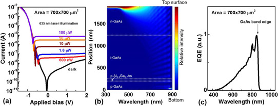
Figure 3: (a) Photocurrent and dark current characteristics of GaAs pin PD on Si as function of applied bias voltage with different optical powers. (b) Simulated optical intensity distribution in active layer as a function of light wavelength. (c) EQE spectrum of fabricated GaAs pin PD on Si as function of light wavelength.
The external quantum efficiency (EQE) increased with illumination wavelength up to near the band edge, above 800nm. The reduced response at shorter, visible wavelengths is attributed to higher reflectance, lack of passivation, and shorter penetration depth. The researchers suggest that passivation could be included in an ARC structure.
Extracted resistance and capacitance parameters suggest that the 3dB bandwidth for response speed of 1900μm2 devices should be around 14.2GHz, “quite close to that of the state-of-the-art device with a similar window size,” according to the team. The researchers add: “We believe that the response speed of our device can reach to that of samples typically fabricated using as-grown GaAs.”
Epitaxial lift-off Wafer bonding Photodetectors AlGaAs MBE
http://dx.doi.org/10.1063/1.4980122
The author Mike Cooke is a freelance technology journalist who has worked in the semiconductor and advanced technology sectors since 1997.


