


- News
24 May 2017
Toward visible and ultraviolet III-nitride lasers on silicon
Researchers in France have created a range of optically pumped III-nitride microdisk lasers on silicon covering a wide range of wavelengths, from 280nm deep ultraviolet to 500nm blue-green/cyan [J. Sellés, Appl. Phys. Lett., vol109, p231101, 2016]. Two types of multiple quantum well (MQW) structure were produced: gallium nitride (GaN) wells with aluminium nitride (AlN) barriers (deep UV), and indium gallium nitride (InGaN) with gallium nitride barriers (violet and blue-green).
The non-alloyed GaN/AlN structures avoid spectral broadening from alloy disorder, compared with more usual AlGaN-based samples. Further, “low interface roughness limits the impact of monolayer fluctuations on the QW transition energy,” according to the team.
The team from Laboratoire Charles Coulomb, Centre de Nanosciences et de Nanotechnologies, Centre de Recherche pour l’Hetero-Epitaxie et ses Applications, Université Grenoble Alpes, and Institut Nanosciences et Cryogénie (INAC), see their work as complementary to the development of infrared integrated photonics for telecommunications. In the case of visible-UV devices, potential applications include bio-chemical analysis and on-chip optical interconnects.
The researchers add: “The broad tunability paves the way to the development of a UV-visible integrated photonic platform embedding microlasers, possibly addressing multiple wavelengths. A further step will deal with the electrical injection, following the recent progresses in electrically injected InGaN lasers on Si-substrates.”
Table 1: Sample active layers.
| Sample | Well/barrier materials | Well thickness (nm) | Number | CW wavelength (nm) |
| GaN-1 | GaN/AlN | 0.7 | 20 | 280 |
| GaN-2 | GaN/AlN | 0.7 | 10 | 290 |
| GaN-3 | GaN/AlN | 1.2 | 10 | 330 |
| GaN-4 | GaN/AlN | 1.8 | 10 | 350 |
| InGaN-1 | In0.12Ga0.88N/GaN | 2.2 | 10 | 417 |
| InGaN-2 | In0.2Ga0.8N/GaN | 2.2 | 10 | 500 |
Ammonia molecular beam epitaxy (MBE) was used on (111)-oriented silicon to produce a range of GaN/AlN and InGaN/GaN structures (Table 1). All the structures were grown on an AlN buffer. The InGaN/GaN structures also included a GaN buffer on top of the AlN. In the InGaN-2 sample, the GaN buffer was silicon-doped to encourage electron injection into the MQW active region.
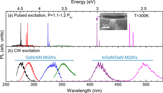
Figure 1: Photoluminescence spectra of six microdisk samples (from left to right, GaN-1 to GaN-4, InGaN-1, InGaN-2); (a) microlaser spectrum above threshold, under pulsed optical pumping; (b) microdisk spectrum in linear regime, under CW excitation. Inset: electron micrograph of 4μm microdisk from InGaN-1 series.
Microdisks were patterned and dry etched before selective under-etch of the substrate to create microdisks (3μm to 12μm diameter) on silicon pedestals (Figure 1). The output was derived from optical pumping with 266nm-wavelength laser light with continuous wave (CW) or pulsed (400ps, 4kHz) operation. The longest-wavelength GaN-4 device was unable to achieve lasing – the researchers attribute this to the quantum-confined Stark effect (QCSE), where electric fields from charge polarization of the III-nitride bonds inhibit electron-hole recombination into photons. GaN-4 contains the thickest wells, compared to the other devices.
Table 2: Microdisk geometries and microlaser characteristics.
| Resonator | Laser | ||||
| Sample | Diameter (μm) | Thickness (nm) | Q | Threshold (mJ-cm2 per pulse) | Wavelength (nm) |
| GaN-1 | 3 | 220 | 4000 | 15 | 275 |
| GaN-2 | 6 | 160 | 2000 | 27 | 290 |
| GaN-3 | 6 | 160 | 2000 | 35 | 330 |
| GaN-4 | 6 | 160 | >1000 | ||
| InGaN-1 | 4 | 515 | 2500 | 3 | 412 |
| InGaN-2 | 5 | 1300 | 2500 | 3 | 47 |
The laser threshold was an order of magnitude smaller for the InGaN/GaN devices, compared with GaN/AlN microdisks (Table 2). “This can be interpreted as the difference between resonant and non-resonant excitation,” the researchers write. “Indeed, the laser energy is below the AlN bandgap and above the GaN bandgap. The 266nm laser pumps the excited states of the GaN/AlN QW, and the 10 QWs can only absorb part of it. On the contrary, the entire pulse energy is absorbed by the GaN barrier in the case of InGaN QWs, leading to a larger carrier density per QW if we assume that all carriers are transferred from the barrier to the well.”
Microdisk lasers GaN AlN barriers InGaN
http://dx.doi.org/10.1063/1.4971357
The author Mike Cooke is a freelance technology journalist who has worked in the semiconductor and advanced technology sectors since 1997.


