


- News
5 May 2017
Ultraviolet photodetection with gallium nitride nanoflowers on silicon
India’s CSIR-National Physical Laboratory (CSIR-NPL) has developed gallium nitride (GaN) nanoflower (NF) structures on silicon as metal-semiconductor-metal ultraviolet (UV) photodetectors (PDs) [Neha Aggarwal et al, Adv. Electron. Mater., vol3, p1700036, 2017]. The team claims: “The reported responsivity is the highest among the GaN UV photodetectors on Si substrates and commercially available silicon-based UV photodetectors.”
The researchers see potential visible-blind UV applications in instrumentation for solar UV monitoring, astronomy, highly secure space-to-space communications, biological sensors, and military uses such as missile detection.
III-nitride materials offer advantages over silicon photodetectors in terms of cut-off wavelength tunability, high thermal stability, high electron saturation velocity, small dielectric constant, and high breakdown field.
The GaN nanoflowers were grown by plasma-assisted molecular beam epitaxy (PAMBE) on a 30nm 825°C aluminium nitride buffer on (111) silicon (Figure 1). The GaN growth began with an 80nm thin layer followed by the nanoflowers. The GaN growth temperature was 730°C.
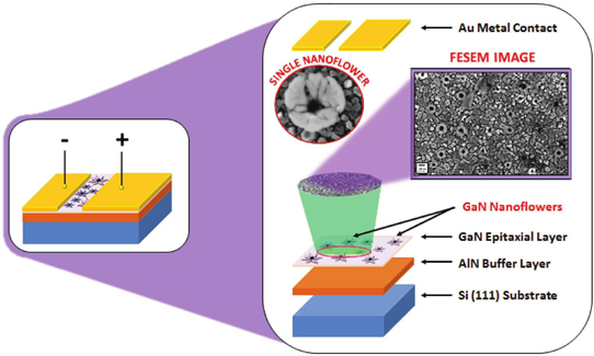
Figure 1: Fabricated device and exploded model representing field emission secondary electron microscopy image of epitaxial GaN film as well as nanoflowers in grown heterostructure.
The photodetector electrodes were gold/chromium (150nm/5nm). The density of nanoflowers was 8.8x10⁷/cm2. The nanoflower structure had a ~200nm diameter at the base, opening up to 300-450nm at the top.
The devices were tested under 325nm UV light. The dark current leakage was attributed to thermionic emission, which increased with the applied bias.
The researchers also found a photocurrent at zero bias. This photocurrent was attributed to the effects of different size electrodes leading to a tilt in the depletion layer inducing charge separation and transport. In particular, a large electrode attracts more photo-generated holes, reducing the barrier height.
The response at zero bias was 132mA/W with 325nm UV of 13mW power. The researchers comment: “The value stated at no bias in the present study is significantly higher than the recently reported self-driven GaN-based photodetector which shows the photoresponsivity of 0.037, 0.083, and 0.104AW−1using different contact electrodes and a flexible self-powered GaN UV photo-switch which possesses responsivities of 0.03 and 0.0116AW−1at the power density of ≈3.5 and 35mWcm−2, respectively.”
The response to 13W UV power pulsed at 10s intervals showed a zero-bias light-to-dark current ratio of 260. The dark current was 90nA. The detectivity – (response (132mA/W) x (active area)1/2) / (2 x (electron charge) x (dark currrent))1/2 – was 2.4x10¹⁰Jones. The rise time was 63ms and the fall time 27ms.
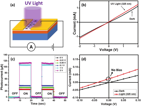
Figure 2: (a) Layout of GaN nanoflower-based UV photodetector device under UV illumination. (b) Current-voltage characteristics under dark and UV light conditions. (c) Time-correlated response of photocurrent generated from device at varying applied bias. (d) Current-voltage characteristics focusing on self-driven behavior (under no bias).
Lower-power illumination of 1mW resulted in a higher response of 10.5A/W. The researchers say that this response level is higher than for commercially available UV photodetectors.
A comparison planar GaN photodetector had a maximum photocurrent of 25.9mA – a 1.5A/W response – at 1V bias under 1mW illumination.
The increased response for GaN NFs is attributed to their higher surface-to-volume ratio, giving a higher rate for absorption of photons and generation of electrons and holes.
The planar device had a noise equivalent power of 60pW/Hz1/2, which is much higher than the 1.2pW/Hz1/2 value found for the photodetectors using GaN nanoflowers. The researchers attribute the lower noise in the GaN nanoflower photodetectors to the reduction of stress and defect states.
GaN UV photodetectors GaN UV Photodetectors Silicon substrates
http://dx.doi.org/10.1002/aelm.201700036
The author Mike Cooke is a freelance technology journalist who has worked in the semiconductor and advanced technology sectors since 1997.


