


- News
10 May 2017
Indium gallium nitride solar cells on non-polar and semi-polar substrates
Arizona State University and University of California Santa Barbara (UCSB) in the USA have compared indium gallium nitride (InGaN) solar cells produced using non-polar, semi-polar and polar substrates [Xuanqi Huang et al, Appl. Phys. Lett., vol110, p161105, 2017]. The non-polar m-plane devices showed the best overall photovoltaic (PV) performance.
InGaN solar cells should be able to convert photons of energy spanning the solar range, with InN having an energy gap of 0.7eV (infrared) and GaN 3.4eV (ultraviolet). In practice, charge polarization of the III-nitride bond leads to strong electric fields in heterostructures arising from spontaneous and strain effects. Growing III-nitride structures in non-polar or semi-polar directions can eliminate or at least reduce these fields and improve performance.
At present, InGaN solar cell demonstrations tend to be in the upper part of the 0.7-3.4eV range, limiting solar conversion efficiencies to a few percent. These high-energy photon converters could be used as top cells in ultra-high-efficiency (>50%) multi-junction solar cells for space and terrestrial concentrating (i.e. focused multi-sun power density) photovoltaics.
Solar cell structures were grown on non-polar m-plane, semi-polar (20-21) and polar c-plane GaN substrates by metal-organic chemical vapor deposition (MOCVD). The layer sequence was 1μm n-GaN, 10nm n+-GaN, 20-period 6nm/10nm In0.2Ga0.8N/GaN multiple quantum well (MQW), 30nm p+-GaN, 120nm p-GaN, and 10nm p+-GaN. The 120nm p-GaN layer was intentionally roughened.
Devices were fabricated with 1mmx1mm mesas, titanium/aluminium/titanium/gold n-contact electrodes, and a nickel/gold p-contact grid with 200μm spacing.
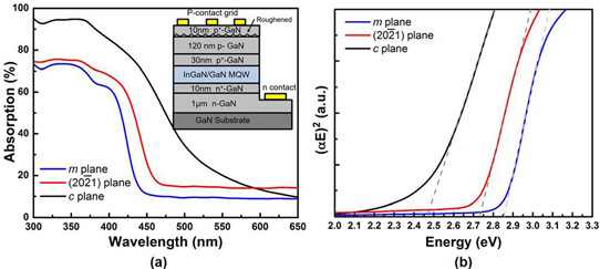
Figure 1: (a) Room-temperature transmission spectra and (b) Tauc’s plots of m-plane, (20-21) plane, and c-plane InGaN MQW solar cells. Inset: cross-sectional schematic of MQW InGaN solar cells.
Table 1: Summary of key device parameters for InGaN/GaN MQW solar cell devices.
| Eg (eV) |
Voc (V) |
Woc (V) |
Jsc (mA/cm2) |
FF (%) |
Peak EQE (%) |
Peak IQE (%) |
|
| m-plane | 2.85 | 2.32 | 0.53 | 0.803 | 55.5 | 39.4 | 61.4 |
| (20-21) plane | 2.73 | 1.92 | 0.81 | 0.736 | 43.2 | 27.1 | 39.6 |
| c-plane | 2.45 | 0.33 | . . . | 0.644 | 29.9 | 21.5 | 25.2 |
Absorption spectra (Figure 1) indicated a red-shift of the bandgap energy (Eg) with increasing polarization in the sequence m-plane, semi-polar, and c-plane (Table 1). Polarization also broadens the absorption edge. Despite the higher cut-off energies, reducing polarization improves other features of solar cell performance such as open-circuit voltage (Voc), bandgap-voltage offset (Woc = Eg/q-Voc, where q is electron charge), short-circuit current density (Jsc), fill factor (FF), and peak external quantum efficiency (EQE) and internal quantum efficiency (IQE) – see Figure 2.
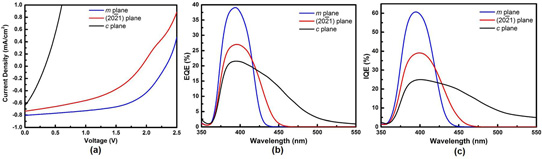
Figure 2: (a) Illuminated J–V curves for m-plane, (20-21) plane, c-plane, InGaN MQW solar cells. (b) EQE and (c) IQE curves for m-plane, (20-21) plane, c-plane InGaN MQW solar cells.
The team comments: “Although the absorption spectra of c-plane solar cell are much higher than non-polar and semi-polar devices, the poor carrier collection efficiency, represented by IQE, leads to a very low Jsc and poor PV performance. Conversely, the non-polar m-plane and semi-polar (20-21) solar cells showed higher EQE despite the lower absorption than that of the polar c-plane device, which can be attributed to improved carrier collection efficiency from reduced polarization-related effect.”
InGaN solar cells InGaN Solar cells MOCVD
http://dx.doi.org/10.1063/1.4980139
The author Mike Cooke is a freelance technology journalist who has worked in the semiconductor and advanced technology sectors since 1997.


