


- News
8 March 2017
Towards polarized white light with tunnel junctions and hybrid growth
University of California Santa Barbara (UCSB) has used a combination of metal-organic chemical vapor deposition (MOCVD) and molecular beam epitaxy (MBE) to produce semi-polar indium gallium nitride (InGaN) devices that emit polarized blue and yellow light [Stacy J Kowsz et al, Optics Express, vol25, p3841, 2017].
The researchers hope that developing these concepts could lead to white light sources with polarized emissions that would reduce power consumption in liquid crystal displays (LCDs). Presently, LCDs use unpolarized backlighting that must be filtered by a polarizer, cutting the energy throughput by more than a half. The use of semi-polar InGaN material can lead to polarized light emission.
The UCSB device consisted of two sequences of multiple quantum wells (MQWs). The bottom sequence comprised a blue light-emitting diode (LED) that optically pumped the top MQW structure to give an added yellow component to the spectrum.
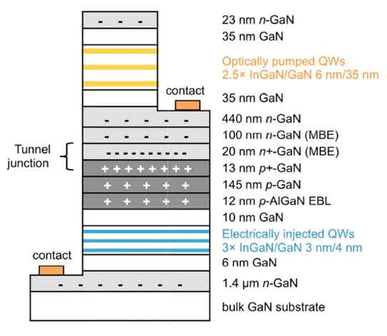
Figure 1: Cross-sectional schematic of device with optically pumped QWs on top of electrically injected QWs.
The LED structure also had a tunnel junction (TJ) layer that was designed to improve current spreading, giving a more uniform current density through the device. “Metal-organic chemical vapor deposition enabled the growth of InGaN QWs with high radiative efficiency, while molecular beam epitaxy was leveraged to achieve activated buried p-type GaN and the TJ,” the team comments.
Current spreading is often achieved with transparent conductive oxides or thin metal layers. However, these options absorb more light than the n-GaN used in the TJ.
The use of a tunnel junction allows the high indium-content InGaN QWs needed for the longer-wavelength yellow emission to be grown at lower temperature, after the high-temperature processes needed for good electrical performance of the blue LED section.
The LED layers were grown by MOCVD. Activation of the p-GaN magnesium doping involved annealing to remove hydrogen that forms a complex with magnesium. Ammonia-assisted MBE was used to create tunnel junctions with sharp p+/n+ interfaces. The MBE n-GaN also blocks hydrogen diffusion from the subsequent MOCVD QWs into the p-GaN layers.
For pure MOCVD, there is a memory effect where growing n-GaN layers after p-GaN results in the silicon-doped n-GaN being contaminated with Mg. Also, oxygen has been found to be beneficial in tunnel junctions – it is thought that the oxygen donates electrons, reducing tunneling distance.
The 600°C Mg-activation annealing was carried out in air, resulting in residual surface oxidation, before transport to the MBE reactor for growth of the tunnel junction. The optically-pumped MQWs were grown by MOCVD after exposing the structure again to air. The second MOCVD sequence was carried out at relatively low temperature except for the first 200nm of n-GaN. Mitsubishi Chemical Corp supplied the 7.5mmx7.5mm free-standing semi-polar (20-21) bulk GaN substrates for the devices.
LEDs were fabricated with a 1.8μm-high 0.1mm2-area circular mesa and a ring injection area for the bottom n-GaN contact layer. The tunnel junction was contacted with a separate 300nm etch of a 3.2μm-radius circular hole at the center of the 0.1mm2 mesa. The contact metals were 450°C-annealed titanium/aluminium/nickel/gold. The backside of the wafer was polished to prevent scattering and to preserve the optical polarization of the light emitted from the strained semi-polar InGaN QWs.
The turn-on voltage for the devices was higher than for LEDs and pn diodes with tunnel junctions produced by UCSB previously using similar techniques. “We expect that improved electrical characteristics for optically pumped and electrically injected TJ devices can be achieved by optimizing the TJ and n-contacts,” the team comments.
The emission consisted of a relatively narrow blue peak at 450nm and a broader peak around 560nm. The mix of components depended on the position of the microscope used to gather emissions. Optical polarization measurements gave an overall ratio of 0.28 along the directions [1-210] and [10-1-4]. The blue LED polarization ratio was 0.2 and the yellow optically pumped MQW ratio was 0.36.
The researchers report: “The polarization ratio of the yellow QWs is greater than the polarization of blue QWs because increasing the InGaN indium content increases strain, which results in separation of the valence bands.”
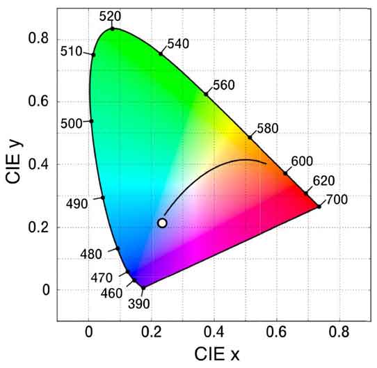
Figure 2: CIE x, y chromaticity diagram with coordinates corresponding to UCSB device spectrum.
The light output from the device has a similar spectral profile as that from ‘white’ LEDs that use a blue light emitter combined with yellow phosphors. On the chromaticity diagram, the 1931 CIE x,y coordinate standard value, (0.23,0.21), lies at the end of the Planckian locus (Figure 2).
The researchers comment: “Increasing the ratio of yellow to blue emission in future devices should enable spatially uniform phosphor-free polarized white light. Moreover, increasing the absorbance, radiative efficiency, and/or number of optically pumped QWs will increase the ratio of yellow to blue emission. Incorporating a dichroic coating with high blue reflectance and high yellow transmittance also will allow for control over the ratio of yellow to blue emission.”
https://doi.org/10.1364/OE.25.003841
The author Mike Cooke is a freelance technology journalist who has worked in the semiconductor and advanced technology sectors since 1997.


