


- News
15 March 2017
Growing quantum dot lasers on microelectronics-compatible silicon
University College London, UK, and Univ. Grenoble Alpes, France, claim the first electrically pumped continuous wave indium arsenide in gallium arsenide (InAs/GaAs) quantum dot (QD) lasers directly grown on industry-compatible nominal silicon (Si) (001) substrates without any intermediate buffers [Siming Chen et al, Optics Express, vol25, p4632, 2017].
The researchers are looking to integration of lasers into silicon photonics devices for cloud-based applications, ‘big-data’ services and enterprise data centers. Often such integration is achieved using wafer bonding, but monolithic growth is expected to result in low-cost, high yield, and large-scale integration of complex optoelectronic circuits. The team used a combination of metal-organic chemical vapor deposition (MOCVD) and molecular beam epitaxy (MBE).
A problem with growing GaAs and other III-V materials on Si is the generation of antiphase boundaries. This can be mitigated with off-axis substrates, but at the cost of reduced compatibility with silicon microelectronics fabrication/integration.
The researchers used microelectronics standard on-axis Si (001) 300mm diameter wafers as substrate for the devices. The MOCVD stage involved an Applied Materials tool.
The silicon surface was prepared by cleaning and annealing at 900°C in hydrogen to reconstruct the surface structure to promote GaAs quality. After the anneal, the temperature was reduced to 700°C in 30 seconds to “freeze” in the surface reconstruction.
A two-step MOCVD was carried out to give 40nm 400°C-500°C GaAs, and 360nm 600°C-700°C GaAs layers. The researchers say that the 400nm GaAs layer on silicon was antiphase-boundary free.
The MBE for the QD laser structure (Figure 1) was carried out in a 3-inch Veeco tool, so the virtual GaAs/Si substrate material had to be diced down to fit into the reaction chamber. The epitaxial design included n-InGaAs/GaAs strained-layer superlattices (SLSs) aiming to block threading dislocations from entering the active region. The cladding layers were Al0.4Ga0.6As, while the 30nm waveguide regions above and below the active region were Al0.12Ga0.88As.
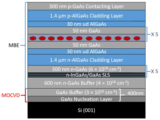
Figure 1: Schematic of QD laser structure grown on on-axis Si (001) substrate.
The “dot-in-well” (DWELL) active region consisted of five sequences of InAs/InGaAs/GaAs dot regions separated by 50nm GaAs spacers. The dot density of uncapped layers was around 3.5x10¹⁰/cm2, according to atomic force microscopy. This compares with 3x10¹⁰/cm2 for dots grown on GaAs substrates.
The material was used to fabricate broad area lasers. Mesa structures were wet etched down to about 100nm above the active region. Further etching reached down to the n-GaAs buffer layer. Titanium/platinum/gold and nickel/germaniumgold/nickel/gold were used for the p- and n-electrodes, respectively. The silicon substrate was thinned to 120μm before cleaving into laser bars.
Testing was carried out on 3mm-long 25μm-wide devices mounted on copper heatsinks. Gold wirebonding was used for electrical connections. The facets were uncoated.
While the series resistance of devices on GaAs/Si and pure GaAs were similar, the QD laser performance was degraded for GaAs/Si compared with pure GaAs substrates. In particular, the threshold current density increased from 210A/cm2 to 425A/cm2 (Figure 2). Also the slope efficiency of the laser on GaAs/Si was reduced to 0.068W/A, compared with 0.12W/A for pure GaAs-based devices. The external quantum differential efficiencies were 7.2% and 12.7% for GaAs/Si and pure GaAs, respectively.
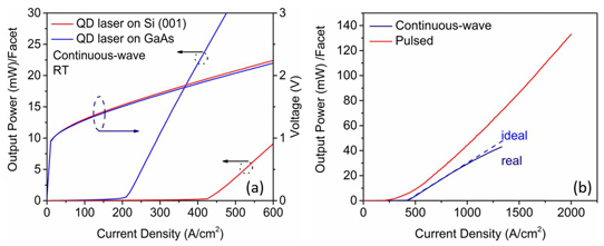
Figure 2: (a) Power-current-voltage (LIV) characteristics comparison of InAs/GaAs QD laser grown on GaAs/Si (001) to reference QD laser grown on native GaAs substrate at room temperature under cw operation. (b) LI comparison of InAs/GaAs QD laser grown on GaAs/Si (001) substrate under cw and pulsed operation conditions at room temperature.
The researchers comment: “Compared with the laser device grown on native GaAs substrate, the degraded device performances for QD laser grown on the Si (001) substrate is related to the defects propagating into the QD active layers.”
The maximum single-facet output power of the QD laser on GaAs/Si was 43mW at 1332A/cm2 continuous wave injection. Pulsed operation increased the maximum to 134mW at 2kA/cm2 injection.
The cw spectrum of the QD laser on GaAs/Si had a peak at 1292nm with 49nm full-width half-maximum (FWHM) at a subthreshold current density of 267A/cm2. Above threshold the FWHM narrowed to around 2.2nm. At higher current, the spectral output showed multiple peaks (i.e. multi-mode behavior).
Temperature-dependent pulse-mode operation saw lasing operation up to 102°C. “To the best of knowledge, this is the first demonstration of QD lasers monolithically grown on exact silicon (001) substrate that lase over to 100°C,” the team writes. The maximum temperature for continuous wave lasing was 36°C. They add: “A next step towards improving the temperature performance and maximum output power will be concerned with reducing the temperature sensitivity and optimizing the extraction of heat from the active region. The well-established strategies to achieve this [are] modulation p-doping of the QDs or/and hard soldering the laser to a high-thermal-conductivity heatsink.”
The team points out that the performance is also down on QD lasers grown on off-cut Si wafers. Further optimization should be possible. The researchers comment: “Nevertheless, good cw performance has been achieved, and the threshold current density reported in the present work has been reduced by more than a factor of two, compared with the very recent achievement of an InAs/GaAs QD laser on on-axis Si (001) substrate with an intermediate GaP buffer layer.”
InAs/GaAs QD lasers MBEs MOCVD
https://doi.org/10.1364/OE.25.004632
The author Mike Cooke is a freelance technology journalist who has worked in the semiconductor and advanced technology sectors since 1997.


