


- News
31 March 2017
Monolithic amber-green-blue nanopillar light-emitting diodes
University of Michigan in the USA has developed monolithically integrated amber-green-blue LEDs (Figure 1) based on strain engineering of indium gallium nitride (InGaN) multiple quantum wells [Kunook Chung et al, Appl. Phys. Lett., vol110, p111103, 2017]. The strain engineering was achieved by etching nanopillars of varying diameter.
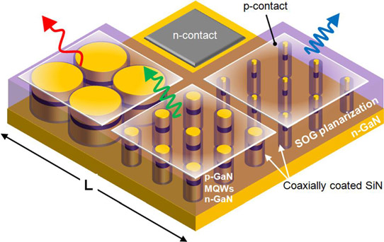
Figure 1: Schematic of top-down fabrication of nanopillar LED arrays with various diameters.
The researchers hope in future to create red-green-blue LEDs using quantum wells with 635nm photoluminescence, giving a viable approach for micro-displays based on such pixel LEDs. Further potential applications include lighting, biosensors, and optogenetics.
In addition to backing from the US National Science Foundation (NSF), Samsung gave fabrication and device design support. In their work, the researchers were keen to develop a chip-scale multi-color LED platform based on existing manufacturing infrastructures.
The epitaxial material was grown by metal-organic chemical vapor deposition (MOCVD) on 2-inch unpatterned sapphire. The light-emitting active region consisted of five 2.5nm InGaN wells separated by 12nm GaN barriers. The electron-blocking and p-contact layers consisted of 20nm aluminium gallium nitride (p-Al0.2Ga0.8N) and 150nm p-GaN, respectively.
The pillars were defined using electron-beam lithography and created by hybrid dry and wet etch processing with a nickel mask. The bulk of the etch was dry, inductively coupled plasma, with the wet stage used to achieve the final diameter and remove damage from the dry step. The etch depth was around 300nm. The etch mask was maintained throughout fabrication to protect the p-GaN surface.
Spin-on-glass was used to planarize the structure after the plasma-enhanced chemical vapor deposition (PECVD) of 50nm silicon nitride to electrically isolate the n- and p-GaN parts of the structure.
The planarized structure was dry etched back to expose the pillar tips. The nickel mask material was removed with nitric acid solution. The p-contact nickel/gold metalization was thermally annealed in air.
The electrical performance of the devices showed low leakage of around 3x10⁻⁷A per pixel at 5V reverse bias. The low leakage is attributed to two factors – flat quantum wells giving low current-crowding effects, and strain-induced confinement of carriers to the center of the nanopillars. The risk of droop effects from the greater current density in the narrower nanopillars is ameliorated by reduced strain, and hence lower quantum-confined Stark effect (QCSE) from electric fields arising from the charge polarization of the chemical bond in III-nitrides.
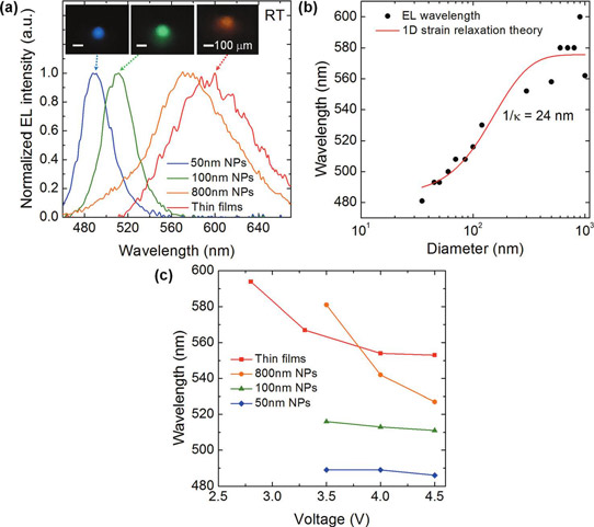
Figure 2: (a) Room-temperature electroluminescence spectra of blue (487nm), green (512nm), orange (575nm) and amber (600nm) emissions obtained from 50nm-, 100nm- and 800nm-diameter nanopillar, and thin-film LED pixels, respectively. Inset: corresponding photographs. (b) Measured emission wavelength as function of nanopillar diameter (black circles) with fitting curve from one-dimensional strain relaxation theory. (c) Dominant peak positions at various applied bias voltages.
The pixels were constructed from pillars with different diameters giving different colors (Figure 2). As the diameter increased, the wavelength became longer and also more variable. The researchers attribute the variability to variations in quantum well thickness across the wafer.
The more relaxed narrow nanopillars also showed less blue-shift in wavelength as the voltage and current injection increased. The blue-shift for 800nm-diameter nanopillar pixels was 40nm between 2.8V and 4V. This is attributed by the team to screening of the strain-dependent piezoelectric field in the wells.
The team foresees stabilizing the output wavelengths of pixels by fixing the bias voltage and varying the intensity by pulse frequency modulation. A test of this idea showed that all the pixel types gave stable wavelengths and relative electroluminescence intensities that varied in a nearly linear manner with the duty cycle of the pulsed signal. The pulse width was 400μs. The pulse frequency varied between 200Hz and 2000Hz.
Integrated amber-green-blue LEDs InGaN InGaN multiple quantum wells MOCVD
http://dx.doi.org/10.1063/1.4978554
The author Mike Cooke is a freelance technology journalist who has worked in the semiconductor and advanced technology sectors since 1997.


