


- News
1 June 2017
Monolithic gallium antimonide-based laser diodes on silicon substrate
Université de Montpellier and III-V Lab in France have developed monolithic quaternary aluminium gallium arsenide antimonide (AlGaAsSb) growth on silicon, producing laser diodes (LDs) emitting at close to the 1.55μm optimum wavelength for fiber-optic telecommunications [A. Castellano et al, APL Photonics, vol2, p061301, 2017]. Normally, GaSb-based laser diodes operate best in the mid-infrared range (longer than 3μm).
The researchers want to see the future development of co-integrated optical data links and data processing electronics on CMOS-compatible platforms. Efficient laser and other light-emitting devices are the most difficult to realize since they require direct-bandgap semiconductors, such as AlGaAsSb alloys, in contrast to the indirect bandgap of silicon.
Growing advanced III-V semiconductors such as AlGaAsSb alloys on silicon suffers from challenges arising from lattice-, thermal- and charge polarity- mismatches. While there has been progress with devices emitting wavelengths away from 1.55μm, previous work of the researchers struggled to create laser diodes at 1.55μm - “these lasers suffered from high-threshold current densities, resulting in poor performances limited to pulsed operation,” the team writes.
The latest laser material was produced using molecular beam epitaxy (MBE) on quarters of 2-inch (001) silicon wafers that were offcut 6° in the [110] direction. The offcut angle was designed to restrict the formation of anti-phase domains arising from charge polarity differences in the chemical bonds between the substrate and III-V compound semiconductors.
The growth was nucleated with four monolayers of 450°C AlSb. The researchers then grew 1μm of GaSb while ramping up to 500°C, 150nm of lattice-matched indium arsenide antimonide (InAs0.92Sb0.08) etch stop/n-contact, and 800nm of 470°C n-GaSb.
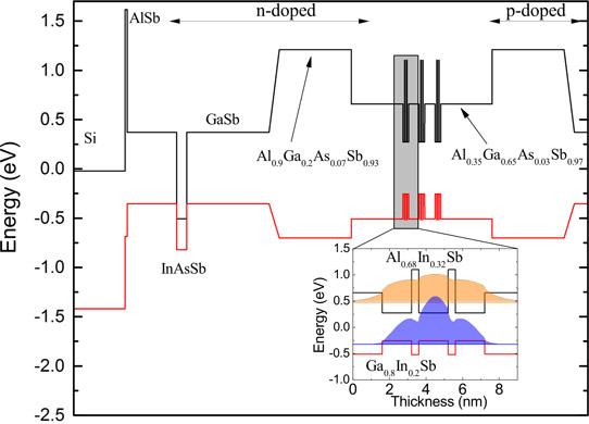
Figure 1: Simulated bandstructure of whole GaSb-on-Si laser heterostructure. Inset: GaInSb/AlInSb composite quantum well details with confined electron and hole levels and wavefunctions.
The rest of the structure was grown at 470°C and consisted of 1.5μm of doped Al0.9Ga0.1As0.07Sb0.93 cladding and 230nm of undoped Al0.35Ga0.65As0.03Sb0.97 waveguide layers above and below the active light-emitting quantum wells. Graded AlGaAsSb layers were used to smooth the band profiles between the buffer and n-cladding, and between the p-cladding and p-GaSb contact layer (Figure 1). Beryllium and tellurim were used for the p- and n-type doping.
The active region consisted of three Ga0.80In0.20Sb/Al0.68In0.32Sb quantum wells separated by 20nm Al0.35Ga0.65As0.03Sb0.97 barriers. The composite well contained 6nm of GaInSb with two insertions of 0.45nm of AlInSb. The strain is estimated at 1.35% relative to the GaSb lattice. The wells have a ‘type-I’ structure where electron and hole wavefunctions overlap by 96.2%, according to simulations. High overlap should lead to better recombination into photons.
The researchers comment: “The confined electron and hole levels are located 180meV and 190meV below the barrier level, respectively (Figure 1). Although sufficient for the holes, this confinement energy is not high enough to totally suppress thermal escape of electrons out of the QWs at room temperature and above.”
The laser diodes were fabricated in a ridge format with gold germanium nickel alloy n-contacts on either side of the ridge and titanium-gold p-contact on top of the ridge. Electrical insulation was provided by photoresist material. The n-contact with the InAsSb layer avoids current flow through the highly defective GaSb buffer region near the silicon substrate, improving performance.
Mirror facets for the laser cavity were obtained by simple cleaving with no optical treatment to increase reflectivity. The devices were mounted epi-side up on copper heatsinks.
Room-temperature pulsed operation of 100μmx1mm broad-ridge laser diodes gave a threshold current density of 1kA/cm2, a value comparable with devices produced on GaSb substrate, according to the researchers. The series resistance was 3Ω and the turn-on voltage 0.8V, close to the value expected from the bandgap.
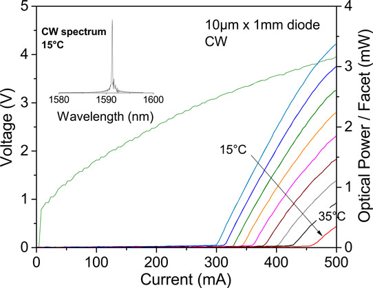
Figure 2: Light output power and voltage versus current curves from 10μmx1mm narrow-ridge laser diode under continuous-wave operation between 15°C and 35°C. Inset: laser emission spectrum at 15°C.
Continuous-wave current injection in 10μmx1mm narrow-ridge laser diodes result in threshold currents of 300mA at 15°C and 450mA at 35°C, corresponding to a characteristic temperature (T0) of 50K (Figure 2). The researchers claim that this is comparable with what is seen in 2μm-wavelength GaSb lasers on silicon and to initial InP-based quantum well devices grown on indium phosphide (InP) emitting near 1.55μm with comparable carrier confinement. At 500mA injection, the narrow-ridge laser diodes output 3.5mW at 15°C and 3mW at 35°C. Higher power could be achieved by increasing current injection towards thermal roll-over. Treating the facets to improve the laser cavity could also boost performance.
At 15°C, the lasing wavelength was 1.59μm, which corresponds to the C/L bands (1530-1565nm/1565-1625nm) for high-performance optical telecoms. [C-band corresponds to the lowest attenuation fiber for dense wavelength-division multiplexing (DWDM). L-band also has low attenuation and allows use of DWDM.]
The variation in performance was represented by a threshold current density that ranges between 1kA/cm2 and 1.5kA/cm2 for the broad-ridge devices at room temperature. The narrow-ridge laser diodes had thresholds between 300mA and 500mA. The researchers comment: “At this stage, we ascribe these variations to different facet qualities of the laser diodes. Indeed, silicon does not spontaneously cleave along the [110] crystal direction as the III-V semiconductors do to form natural facets.”
Monolithic quaternary AlGaAsSb Laser diodes
http://dx.doi.org/10.1063/1.4983389
The author Mike Cooke is a freelance technology journalist who has worked in the semiconductor and advanced technology sectors since 1997.


