


- News
7 June 2017
Improving isolation of gallium nitride transistors on silicon-on-insulator
Researchers based in Belgium and Finland have used silicon-on-insulator (SOI) substrates to improve the electrical isolation of p-type gallium nitride (p-GaN) high-electron-mobility transistors (HEMTs) [Xiangdong Li et al, IEEE Electron Device Letters, published online 16 May 2017].
The team, from imec and KU Leuven in Belgium and Okmetic Oy in Finland, sees electrical isolation as being vital for monolithic power circuits such as half-bridge layouts with transistors biased at significantly different levels. Such isolation is difficult when devices are placed on a common conductive substrate. At present, isolation is achieved by multi-chip modules that involve increased production complexity and cost.
The researchers comment: “This work demonstrates that, by using GaN-on-SOI in combination with trench isolation, it is very promising to monolithically integrate GaN power systems on the same wafer to reduce the parasitic inductance and die size.”
It has also been found that growing GaN on SOI can result in higher-quality material, an effect that is attributed to the more compliant nature in terms of stress and strain of the insulator component of the wafer – silicon dioxide (SiO2).
The 200mm-diameter SOI wafer consisted of a 1070μm (100) Si handle, 1μm buried SiO2, and 1.5μm (111) Si device layer. The SiO2 thickness gave a balance between high breakdown voltage and low thermal resistance.
Metal-organic chemical vapor deposition (MOCVD) resulted in 200nm aluminium nitride (AlN) nucleation, a 2.6μm (Al)GaN superlattice buffer, a 300nm GaN channel, a 12.5nm Al0.25Ga0.75N barrier, and 80nm of p-GaN. After deposition the p-GaN layer was annealed in-situ in nitrogen to activate the magnesium doping, giving a hole concentration of ~1018/cm3.
The (Al)GaN buffer was designed to control stress and avoid wafer warpage (<50μm). Surface roughness was 1.4nm root-mean-square, according to atomic force microscopy.
The enhancement-mode (i.e. normally-off) p-GaN HEMTs (Figure 1) were fabricated with gold-free processing. Future integration with silicon electronic circuitry would need to eliminate gold from the production process since the element poisons carrier transport in silicon.
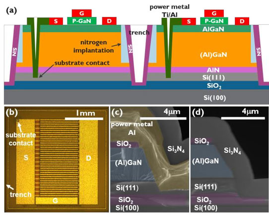
Figure 1: (a) Schematic cross-section of enhancement-mode p-GaN HEMT, (b) top view of fabricated device, and cross-section secondary-electron micrographs of (c) substrate contact and (d) trench isolation fabricated on 200mm GaN-on-SOI.
The gate stack consisted of titanium nitride on p-GaN. Horizontal isolation was achieved with nitrogen ion implantation. A 50μmx50μm substrate contact was created by etching through to the Si(111) device layer and sputtering titanium/aluminium, connecting the substrate with the ohmic source contact.
The device was completed with etching of a 20μm-wide isolation trench reaching down to the buried oxide and with deposition of a passivation layer. The trench isolation was found to have a horizontal breakdown voltage around 700V at 150°C. The vertical breakdown of the buried oxide was around 500V at the same temperature.
The gate was 36mm wide and 0.8μm long. The distances between the gate and the source and drain were 0.75μm and 6μm, respectively.
The gate threshold voltage was around +1.6V. A comparison device on non-SOI silicon had the same threshold. The comparison device did not have the substrate contact or trench isolation. The on-resistance of the comparison device was 10.6Ω-mm, and that of the SOI p-GaN HEMT was only slightly higher at 10.8Ω-mm at 0.1V drain bias and 7V gate potential. The maximum drain current with 7V gate potential was 9A across the 36nn gate width, for both devices.
With the gate at 0V, the off-state breakdown for both devices was around 600V for 1μA/mm leakage. The researchers say that this gives sufficient margin for 200V-rated applications.
Where the SOI device improved on the comparison device was in the effectiveness of the electrical isolation. This was tested by biasing the substrate of the neighboring device between -200V and +200V (Figure 2). In particular, the SOI device’s threshold voltage was stable over the bias range, while that of the HEMT on silicon varied by a few volts.
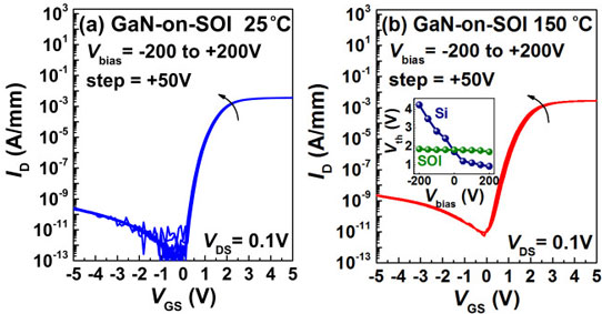
Figure 2: Evaluation of device isolation on GaN-on-SOI by measuring transfer characteristics while simultaneously biasing neighboring Si(111) device layer at different voltages at (a) 25°C and (b) 150°C. Inset: threshold Vth as function of different substrate bias at 150°C.
“With the demonstrated high-quality device isolation, it is very promising to achieve monolithic integration of GaN power system on GaN-on-SOI, and further explore the potentials of GaN in the field of high-power applications,” the team writes.
GaN GaN HEMTs SOI substrates MOCVD
https://doi.org/10.1109/LED.2017.2703304
The author Mike Cooke is a freelance technology journalist who has worked in the semiconductor and advanced technology sectors since 1997.


