


- News
26 July 2017
Towards gallium nitride integration with silicon CMOS
Researchers in the USA have developed gallium nitride (GaN) high-electron-mobility transistors (HEMTs) fabricated on 200mm-diameter silicon-on-insulator (SOI) substrates with multiple crystal orientations [Ko-Tao Lee, et al, IEEE Electron Device Letters, published online 27 June 2017]. The team from IBM’s T. J. Watson Research Center, Massachusetts Institute of Technology (MIT), Veeco Instruments Inc, and Columbia University, hope the work will lead to heterogeneous integration of GaN power transistors with high-speed complementary metal-oxide-semiconductor (CMOS) devices.
Silicon CMOS is not compatible with high-voltage or intense power density applications such as photovoltaic inverters, electric vehicle charging, and DC power transmission. “Because GaN is better suited for these applications, co-integration of GaN with Si may provide a pathway for both high-power and high-performance applications on a single chip,” the researchers write.
The substrates consisted of 750μm silicon in the (111) crystal orientation, 145nm buried oxide (SiO2) and 80nm Si (100). The Si (111) was used for the growth of GaN, while the Si (100) gives optimum performance for CMOS devices. Thermal oxidation of the Si (100) surface reduced the 80nm layer to 40nm. The researchers point out that this is the preferred thickness for state-of-the-art 14nm-node CMOS.
Reactive ion etch was used to expose Si (111) window regions up to 200μmx200μm for selective GaN growth (Figure 1). The total GaN coverage was less than 50%, restricting bowing/warpage to within that needed for silicon CMOS specifications (less than 50μm bow, for example).
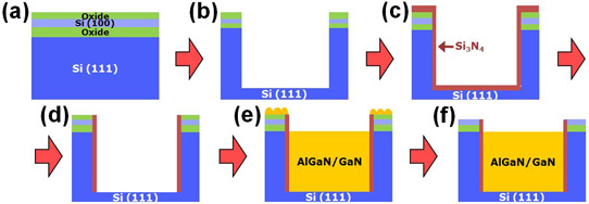
Figure 1: Hybrid-oriented SOI substrate with top Si (100) and bottom Si (111) preparation for MOCVD growth: (a) CVD-SiO2 growth, (b) dry etching to expose Si (111) plane, (c) Si3N4 growth via CVD as isolation and diffusion barrier, (d) Si3N4 removal via dry etch to expose Si (111) plane, (e) AlGaN/GaN HEMT growth, (f) CVD-SiO2 removal via chemical-mechanical planarization.
The team comments: “The need for large-periphery high-power devices can potentially be achieved by combining multiple small patterned GaN devices. Once this approach is successful, this technology can extend the GaN-on-Si co-integration platform to high-power applications.”
Silicon nitride (Si3N4) was deposited as a spacer on the window sidewalls, electrically isolating the GaN and Si (100) regions. The silicon nitride also provided a diffusion barrier, stopping Ga and Si atoms from doping the adjoining regions.
The GaN and AlGaN material was grown by metal-organic chemical vapor deposition (MOCVD): 130nm 1050°C AlN nucleation, 1.5μm 1035°C GaN buffer/channel, and post-growth ramp down to 985°C to “facilitate unintentional [?] carbon doping”. MOCVD for HEMTs added a 1nm AlN spacer, a 20nm Al0.25Ga0.75N barrier, and a 3nm GaN cap.
A GaN layer grown on a Si (111) control wafer under the same conditions was only 0.6μm thick, less than half that of 1.5μm layer in the SOI Si (111) regions. The increased thickness for the selective area growth was attributed to ‘micro-loading effects’ from the confined space of the Si (111) regions.
Standard HEMTs were produced with 3μm gate length and 3μm spacing between the gate and source and drain regions.
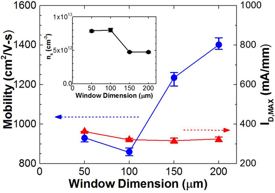
Figure 2: Electron mobility and drain current of GaN HEMTs from various window dimensions. Inset: corresponding carrier density (ns) as a function of window dimension.
While the mobility varied according to the size of the window regions, declining with reduced size, the maximum drain current for the HEMTs was roughly constant (Figure 2). “The decline in electron mobility with decreasing window dimension is believed to be related to higher strain relaxation in smaller windows,” the researchers explain.
Breakdown voltage was reduced with the smallest 50μmx50μm windows (~40V versus ~80V for larger windows), which the researchers suggest could be due to defects at the GaN/Si3N4 sidewalls. By contrast, current collapse increased for the largest 200μmx200μm windows (~25% versus less than ~6% for smaller windows). The quiescent state for the collapse measurements was -3V gate potential and 10V drain bias. The pulse width was 500ns. A 100μmx100μm window device demonstrated a collapse less than 2%. The researchers give 25% collapse as being typical for HEMTs on ‘bulk’ GaN.
The researchers comment: “The current collapse appears to correlate with the strain relaxation in patterned GaN, which is lower in smaller windows. Although the exact mechanism for this phenomenon needs further investigation, we believe that an interplay between defects and strain in patterned GaN dictates the observed current collapse behavior.”
GaN HEMTs GaN HEMTs SOI substrates MOCVD
https://doi.org/10.1109/LED.2017.2720688
The author Mike Cooke is a freelance technology journalist who has worked in the semiconductor and advanced technology sectors since 1997.


