


- News
5 July 2017
Smart stacking III-V on crystal silicon solar cells to boost conversion
Japan’s National Institute of Advanced Industrial Science and Technology has used palladium nanoparticle (Pd NP) arrays to connect crystalline silicon (c-Si) and III-V tandem solar cell stacks, resulting in high conversion efficiency [Hidenori Mizuno et al, Appl. Phys. Express, vol10, p072301, 2017]. The researchers term the technique ‘smart stack’.
While silicon solar cell technology offers the advantages of mature mass production and low cost, single-cell silicon devices are theoretically limited to conversion efficiencies less than ~29%. Using tandem structures with III-V thin-film subcells above c-Si cells could extend this performance.
The researchers used a simple aluminium back surface field (BSF)-type c-Si cell, based on a 400μm-thick double-side mirror polished, p-type Si (100) substrate. An n+-Si surface layer was created using thermal diffusion of phosphoryl chloride (POCl3). The p+-Si BSF was achieved through screen-printing and firing of aluminium paste.
The structure was prepared for smart-stack bonding with the indium gallium phosphide/gallium arsenide (InGaP/GaAs) (0.35μm/0.5μm) thin-film cell by creating a Pd NP array in a self-assembled polystyrene-block-poly(2-vinylpyridine) template. The gap between the GaAs and silicon layers was found to be uniformly around 10nm.
The InGaP and GaAs absorber layer thicknesses were designed to give relatively matched currents for the three subcells from AM1.5g standard solar illumination – 10.7mA/cm2 from InGaP, 10.7mA/cm2 from GaAs, and 10.2mA/cm2 from Si. Matching currents is very important for high efficiency.
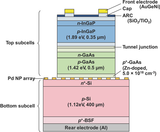
Figure 1: Schematic cross-section of InGaP/GaA//Si (“/” is tunnel junction, “//” is Pd NP smart stack) triple-junction cell.
The completed structure (Figure 1) included a gold-germanium-nickel (AuGeNi) front electrode and silicon dioxide/titanium dioxide (SiO2/TiO2) anti-reflective coating (ARC).
The researchers comment: “It should be emphasized that no additional heat treatment was necessary to improve the bonding quality (lower the interfacial resistance), which is usually required with other bonding-based fabrication of two-terminal tandem cells.”
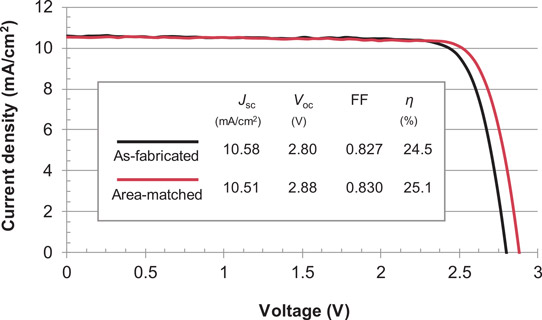
Figure 2: Current density-voltage (J–V) characteristics of as-fabricated (before-cutting, black curve) and area-matched (after-cutting, gray curve) InGaP/GaAs//Si cells.
PV measurements with AM1.5g solar spectrum illumination (1 sun, 100mW/cm2) showed 24.5% conversion efficiency η (Figure 2). The researchers found that the open-circuit voltage (Voc) was down on what was expected from measurements on separate cells: “This could be attributed to the shading of the c-Si bottom subcell because, in this situation, unfavorable migrations of photo-generated carriers to unilluminated regions could easily occur. This would lead to an increased dark current and recombination probability, and thereby a decreased Voc.”
The high fill factor (FF) of 0.827 was attributed to the low resistance interface between the silicon and GaAs given by the Pd NP array.
To improve the performance by tackling the shading issue, the researchers used a dicing saw to remove excess regions of the c-Si bottom cell. This increased Voc, although it reduced the short-circuit current density (Jsc) somewhat. The researchers say that the current degradation was not significant – indeed, the FF increased to 0.830 and the conversion efficiency was enhanced to 25.1%. The team adds that the improved performance after using the dicing saw strongly supports “the hypothesis that smart stack cells are durable enough to withstand rather severe semiconductor processes”.
The researchers say that they consider the observed performance as being close to the best achievable for the types of subcells used. “Higher-efficiency smart stack cells will require development of high-quality, thicker InGaP/GaAs cells, advanced c-Si cells, and tricks for current matching between them, which is actively underway in our group,” the team adds.
Palladium nanoparticle InGaP GaAs
https://doi.org/10.7567/APEX.10.072301
The author Mike Cooke is a freelance technology journalist who has worked in the semiconductor and advanced technology sectors since 1997.


