


- News
13 July 2017
Amber quantum wells on indium gallium nitride pseudo-substrate
University Grenoble Alpes and Soitec S.A. in France have used layer transfer techniques to create indium gallium nitride on oxide/sapphire (InGaNOS) pseudo-substrates [A. Even et al, Appl. Phys. Lett., vol110, p262103, p2017]. The pseudo-substrates enabled the researchers to grow high-indium-content InGaN multiple quantum wells (MQWs) with strong long-wavelength photoluminescence in the amber part of the spectrum (594nm). Similar MQWs produced on conventional GaN/sapphire templates generally only produce weak photoluminescence. The hope is to apply such techniques in creating high-efficiency green and even amber light-emitting diodes (LEDs) from III-nitride semiconductor materials.
The researchers comment: “The reduced strain, due to a relaxed InGaN substrate, leads to a reduction in the compositional pulling effect and therefore to an enhancement in the indium incorporation rate. In addition, as the a-lattice mismatch between the well and the buffer layer is decreased, the internal electric field should be reduced for the same emission wavelength compared to a conventional LED. This gives the possibility of increasing the well width in order to reduce the efficiency droop of LEDs with a long emission wavelength.”
The donor material consisted of metal-organic vapor phase epitaxy (MOVPE) InGaN grown on a GaN/sapphire template. Three InGaN compositions were produced with varying a-lattice parameters: 3.190Å, 3.200Å, and 3.205Å, as determined by x-ray diffraction (Figure 1). The indium content for the largest lattice parameter is estimated at around 8%. Sample A’s lattice parameter was comparable to that of free-standing GaN. The researchers comment: “As it is difficult to incorporate a large amount of indium into a thick continuous layer on a GaN template, the maximum InGaNOS average In content is limited to 8%.”
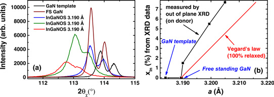
Figure 1: (a) In-plane XRD spectra [2θχ-φ scan on the (300) reflection] of three InGaNOS substrates [3.190Å (blue curve), 3.200Å (green curve), and 3.205Å (red curve)] and with GaN references [GaN free-standing substrate (brown curve) and GaN template on sapphire (black curve)]. (b) Indium content measured by out-of-plane XRD as a function of the a-lattice parameter inferred from (a) spectra (black curve) and corresponding Vegard’s law (red curve).
The InGaN layer was transferred to sapphire using SOITEC’s Smart Cut technology. Hydrogen ion implantation creates a weakened region inside the donor material. The donor wafer was then bonded to sapphire using silicon dioxide layers on the donor and target substrates. Heat treatment then splits away the donor GaN/sapphire template at the hydrogen implantation region.
The process resulted in an InGaN layer on buried oxide and sapphire handle, giving an InGaNOS pseudo-substrate. The InGaN layer was patterned and etched into 800μmx800μm or 500μmx500μm square mesas, and then subjected to successive thermal treatments in an effort to relax the strained InGaN crystal structure. “The challenge of this process is to get a uniform relaxed InGaN layer while keeping a flat surface,” the team reports.
Multiple quantum wells (MQWs) were grown by MOVPE on a further 150nm metal-polarity InGaN buffer: 5x 3nm InGaN wells separated by 8nm InGaN barriers. Photoluminescence measurements suggested indium contents in the buffer layers of between 6% and 7%, depending on the indium content of the InGaNOS pseudo-substrate. Using the same buffer growth conditions resulted in 4%-indium-content InGaN on GaN templates. The barriers were designed to have the same composition as the buffer.
A further aspect of buffer growth on InGaNOS pseudo-substrate was narrowing of x-ray diffraction rock-curve peaks (395 arcsec) compared with material grown on GaN templates (414 arcsec). The researchers suggest that this is associated with a reduction in the density of V-pits that tend to form at high indium concentrations.
The quantum wells were produced with varying growth conditions designed to achieve different emission wavelengths. ‘Sample A’ had standard blue-emitting wells grown at 750°C with 0.1μm/hour growth rate. ‘Sample B’ was grown at 20°C lower temperature, increasing indium incorporation. For ‘Sample C’, the growth rate was increased by a factor of three in addition to lower temperature.
Photoluminescence from the three types of MQW structure (A-C) on the three types of InGaNOS pseudo-substrate showed red-shifts compared with MQWs on GaN templates (Figure 2). Sample A gave blue to green emissions, sample B green, and sample C green to amber.
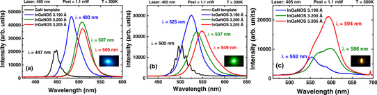
Figure 2: Photoluminescence spectra at 300K of full InGaN heterostructures on InGaNOS (a) samples A, (b) samples B, and (c) samples C (blue curve is related to InGaNOS 3.190Å, green curve to 3.200Å, red curve to 3.205Å, and black curve to reference sample). Insets: pictures of emission under laser excitation from InGaNOS samples of (a) 3.190Å blue luminescence, (b) 3.200Å green luminescence, and (c) 3.205Å amber luminescence.
The sample C series does not include MQWs grown on GaN templates since such growth conditions do result in significant photoluminescence.
The Sample C MQW spectra seem to contain separate green and amber components. With the 3.190Å InGaNOS pseudo-substrate, the green component dominates, while for the other pseudo-substrates the amber light becomes more prominent.
The researchers suggest that the high-indium-content InGaN in the wells may suffer phase separation, with regions of high and low concentration giving, respectively, amber and green emission. The largest-lattice-parameter InGaNOS pseudo-substrate gave roughly twice the photoluminescence intensity of the middle parameter sample at 594nm wavelength.
The photoluminescence spectra of all the samples were relatively broad. The researchers suggest this is due to thickness fluctuations of the wells, as seen in high-resolution transmission electron microscopy.
Internal quantum efficiency (IQE) was estimated, based on measurements at 10K and 300K. The researchers report that B samples on 3.200Å InGaNOS without optimization had 31% IQE at 536nm and 10% at 566nm.
InGaNOS pseudo-substrates MOVPE InGaN
http://dx.doi.org/10.1063/1.4989998
The author Mike Cooke is a freelance technology journalist who has worked in the semiconductor and advanced technology sectors since 1997.


