


- News
3 January 2017
Avalanche photodiode with photomultiplier-like performance
Researchers in China and France have developed photomultiplier tube (PMT)-type performance from avalanche photodiodes (APDs) that implement periodically stacked structures (PSSs) of gallium nitride (GaN) and aluminium nitride (AlN) [Jiyuan Zheng et al, Appl. Phys. Lett., vol109, p241105, 2016]. The PSS APD had a record high gain of order 104 with noise factor as low as 500 and ionization coefficient of 0.05, according to the researchers. The highest gain for silicon APDs in linear mode is about 100.
The team from Tsinghua University in China, CNRS-CRHEA (Centre de Recherche sur L'Hétéro-Epitaxie et ses Applications-Centre National de la Recherche Scientifique) in France and Institute of Semiconductors, Chinese Academy of Sciences in China used Monte Carlo simulations to develop the APD. By employing the PSS technique, the team hoped to avoid inter-valley scattering that reduces the performance of conventional APDs.
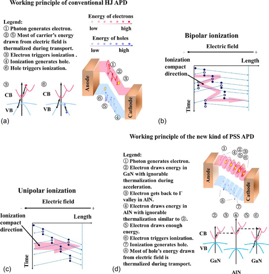
Figure 1: Motivations of design: (a) carrier transport in conventional heterojunction APDs under electric field, (b) bipolar ionization proceeding along two opposite directions and (c) unipolar ionization proceeding along single direction. (d) Carrier transport in GaN/AlN PSS APDs.
The PSS technique (Figure 1) enhanced the multiplication effect for electrons, but not for holes. This made the APDs unidirectional in terms of response to incoming photons and the resulting avalanche electrons. Suppression of hole avalanche reduced the potential for breakdown events.
PMTs are a vacuum tube technology used to measure low lighting conditions, including in single-photon experiments. Researchers would like to replace bulky, fragile PMTs with compact, robust solid-state devices based on semiconductors.
A prototype structure with alternate 20x 10nm/10nm layers of GaN/AlN were fabricated into PSS APDs. The structure was grown by molecular beam epitaxy (MBE) on AlN/sapphire templates supplied by Suzhou Nanowin Science and Technology Co Ltd. After depositing 50nm AlN on the AlN template, the p-i-p-i-n structure was grown with separated absorption (I-GaN and multiplication (I-AlN/GaN) layers (Figure 2).
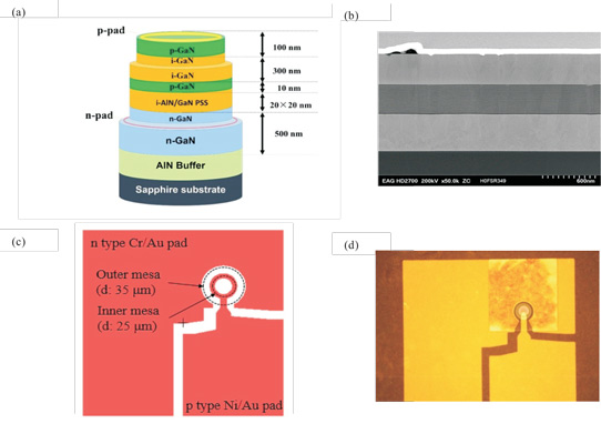
Figure 2: Design and fabrication of GaN/AlN PSS APD: (a) epi-structures, (b) cross-sectional transmission electron micrograph of epitaxy layers, (c) device processing design. (d) Top-view micrograph of practical device.
A double mesa structure with inner diameter of 25μm and outer diameter of 35μm was etched by inductively coupled plasma. The light absorption occurs through the top of the inner mesa. Further fabrication included plasma-enhanced chemical vapor deposition (PECVD) of silicon dioxide and ohmic contact formation – p-type nickel/gold and n-type chromium/gold. Electrode pads were gold.
The external quantum efficiency (EQE) of the devices increased with bias voltage, unlike traditional APDs (Figure 3). The saturation of EQE occurred around 104, representing 14 2x multiplication stages. The probability for electron-triggered ionization is estimated at 70% per period. This is close to the 80% predicted by Monte Carlo simulation.
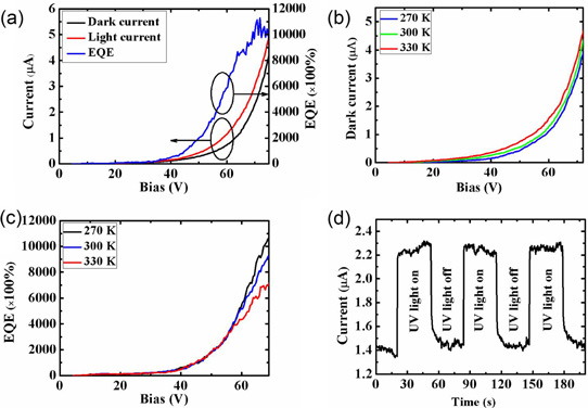
Figure 3: (a) Current-voltage and EQE-voltage curves; (b) revers-biased dark current curves tested under different temperatures. (c) Temperature dependence of EQE-V curves. (d) Device under constant bias responding to ultraviolet 325nm laser light switching on and off.
The researchers believe higher gain could be achieved by increasing the number of GaN/AlN stacks in the PSS region.
By using III-nitride alloys with different electronic band structures, the researchers believe that devices with various working wavelengths ranging from infrared to ultraviolet could be realized using inter-band or inter-subband transitions. They also see electronic amplifiers being developed based on the same carrier multiplication mechanism.
http://dx.doi.org/10.1063/1.4972397
The author Mike Cooke is a freelance technology journalist who has worked in the semiconductor and advanced technology sectors since 1997.


