


- News
11 January 2017
Back-reflector for gallium indium nitride arsenide solar cells
Tampere University of Technology in Finland has developed a back-reflector structure for gallium indium nitride arsenide (GaInNAs) solar cells with a view to their incorporation in high-conversion-efficiency triple-junction structures [Timo Aho et al, Appl. Phys. Lett., vol109, p251104, 2016]. The team estimates that their back-reflectors could lead to 28% increased short-circuit current (Jsc) under concentrator-type illumination.
There are difficulties in providing GaInNAs layers with low enough background doping. This limits the thickness of the absorber layer. By applying a reflector to the back surface of the structure one can effectively double the photon path length in the absorber region for higher-efficiency energy extraction.
The researchers see potential application in space and concentrator photovoltaic systems with high power-to-mass ratio, radiation durability, and high efficiency. GaInNAs with around 4% nitrogen content is seen as being suitable for harvesting longer-wavelength (1400nm) photons with energy around 0.9eV. In multi-junction structures, higher-energy photons are filtered out by the upper layers of the device.
Since charge is conserved, currents in multi-junction structures must be equal throughout the cell. The team comments: "The results enable current-matching for GaInNAs materials with a high amount of N corresponding to bandgaps below 0.9eV, ultimately allowing the development of lattice-matched solar cells with more than three junctions." They also report low contact resistivity and that none of the samples exhibited notable peeling of metals in adhesion tests. The researchers add: "Moreover, no discernible diffusion of the metals into the semiconductor was observed after thermal annealing at 200°C."
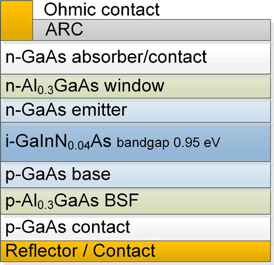
Figure 1: Generic test structure of back-surface reflector cell. Light enters from n-GaAs side.
The solar cells were fabricated from material grown by molecular beam epitaxy (MBE) – see Figure 1. Four mirror structures were compared with metals deposited by electron-beam evaporation (Table 1). The main mirror type was an unannealed combination of silver/copper/nickel/gold (Ag/Cu/Ni/Au) with varying thicknesses (including zero). The Ag, Cu and Au components give almost ideal reflectivity for wavelengths longer than 800nm. A benchmark cell replaced the mirror layers with an annealed titanium/gold (Ti/Au) ohmic contact.
Table 1: Mirror structures.
| Mirror | Structure | Thicknesses |
| 50nm Ag/Cu | Ag/Cu/Ni/Au | 50nm/100nm/10nm/50nm |
| 30nm Ag/Cu | Ag/Cu/Ni/Au | 30nm/100nm/10nm/50nm |
| 10nm Ag/Cu | Ag/Cu/Ni/Au | 10nm/100nm/10nm/50nm |
| Cu | Cu/Ni/Au | 100nm/10nm/50nm |
| Au | Au | 100nm |
| Ti/Au | Ti/Au | 50nm/100nm |
The Ag was used both as a reflector and diffusion barrier, aiming to stop Cu from mixing with and poisoning the semiconductor material and reducing open-circuit voltages. In addition to reflecting light, the Cu acted as a high-conductivity current spreader. The Ni was used as an adhesive layer between the Cu and Au. The final Au layer protected the mirror and acted as a bonding surface.
The top ohmic contact consisted of indium, while the light entered through a titanium dioxide/silicon dioxide bilayer anti-reflective coating (ARC).
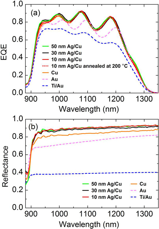
Figure 2: (a) EQE of GaInNAs solar cells with various back-surface reflectors and (b) reflectance of double-side-polished semi-insulating GaAs samples with back-surface reflectors and without ARC.
The external quantum efficiency (EQE, Figure 2) was improved by using Ag/Cu, Cu or Au mirrors (~0.9 peak) over that of using a Ti/Au ohmic bottom contact (~0.7 peak). This was based on a 52% improvement in reflectivity near the band edge, comparing 10nm Ag/Cu with Ti/Au. The Ag/Cu mirrors gave similar performance. The Au reflector had performance intermediate between the Ag/Cu and Ti/Au structures. Also, thermal annealing of the 10nm Ag/Cu mirror at 200°C for 90 seconds did not significantly affect the EQE, indicating some latitude in processing thermal budget.
The short-circuit current (Table 1) was deduced from the EQE measurements under atmospheric mass AM1.5 (sun zenith angle 48.2°) and AM0 (space) simulated conditions. The AM1.5 simulated spectrum was also separated into those suitable for flat-panel (AM1.5G) and concentrator ('direct', AM1.5D) systems. The model assumed a thick GaAs filter on top of the solar cell.
The researchers comment: "The solar cell with the 30nm Ag/Cu reflector exhibited a Jsc value of ~14mA/cm2 at AM1.5D (1000W/m2 ), which is 28% higher compared to the reference solar cell with the Ti/Au reflector. These values are similar to the current that can be generated by GaInP/GaAs top cells, which is ~14mA/cm2 at AM1.5D (1000W/m2 )."
The team further expects a 10-percentage-points higher conversion efficiency for an Ag/Cu reflector bottom cell compared with Ti/Au in an optimized GaInP/GaAs/GaInNAs triple-junction solar cell under ~1000xAM1.5D illumination. This would raise conversion efficiencies from around 35% to 45%.
GaInNAs solar cells GaInNAs Solar cells GaAs MBE
http://dx.doi.org/10.1063/1.4972850
The author Mike Cooke is a freelance technology journalist who has worked in the semiconductor and advanced technology sectors since 1997.


