


- News
27 January 2017
Increasing light output power from gallium nitride LEDs with p-trenches
Seoul National University and Samsung Electronics Co Ltd in South Korea have used trenches filled with p-type gallium nitride to increase the output power of indium gallium nitride (InGaN) light-emitting diodes (LEDs) [Garam Kim et al, Appl. Phys. Lett., vol110, p021115, 2017].
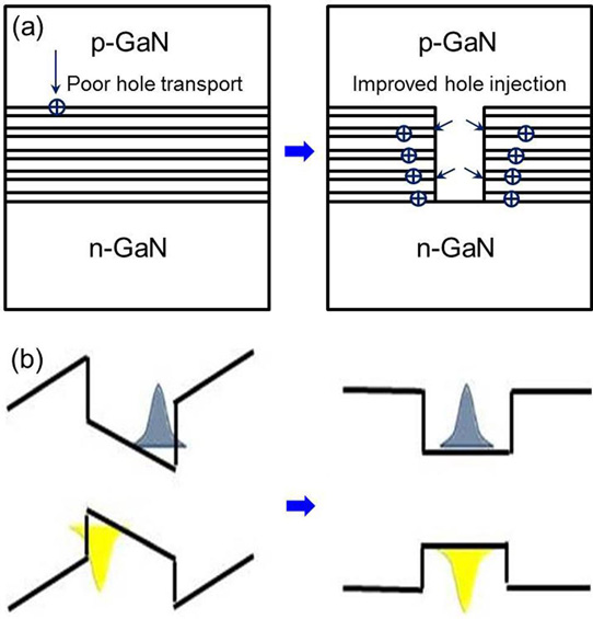
Figure 1: (a) Hole distribution in MQW of conventional LED and p-type trench LED. (b) Energy band structure in MQW when strain is present or eliminated.
The aim of the trenches was to allow holes to enter multiple quantum well (MQW) structures more effectively. In conventional LEDs, holes from the top p-GaN contact layers tend to only get as far as the top well, meaning that not much light is emitted from the lower wells. With trenches, the researchers hoped to increase the numbers of holes injected into the deeper parts of the device (Figure 1a).
It was also hoped that splitting up the strained material with trenches would reduce piezoelectric fields in MQW structures arising from charge polarization of the III-nitride bonds. The strain is due to lattice mismatching between the GaN and InGaN crystal structures.
The (piezo-)electric field tends to pull electrons and holes apart, reducing wavefunction overlap and conversion into photons (Figure 1b). This is commonly referred to as the quantum-confined Stark effect (QCSE). The effect can be avoided by growing material in semi-polar or non-polar crystal orientations, but that often requires the use of prohibitively expensive free-standing or bulk GaN substrates.
Poor hole transport is among the many issues that are thought to contribute to efficiency droop at high current injection. With most electron-hole recombination occurring in one or two wells, the onset current for non-radiative 'Auger'-like processes is reduced. Further, the probability for electron overflow into the p-GaN contact layer is increased.
Trenches were defined by electron-beam lithography on 3nm/12nm InGaN/GaN multiple quantum wells grown by metal-organic chemical vapor deposition (MOCVD) on c-plane sapphire. The active region emitted blue light. The lithography was carried out on a 100nm coating of polymethyl methacrylate (PMMA) resist. The patterning into trenches was transferred into the MQW structure by inductively coupled plasma etch. The p-type GaN filling the trenches was laterally grown at 950°C temperature and 200Torr pressure.
The researchers also tried a selective wet etch method to create the trenches, using potassium hydroxide in ethylene glycol at 165°C. The selection was on threading dislocations, rather than being defined by lithography.
The electroluminescence of the structures was tested by applying an indium tin oxide (ITO) current-spreading layer. The metal contact was chromium/nickel.
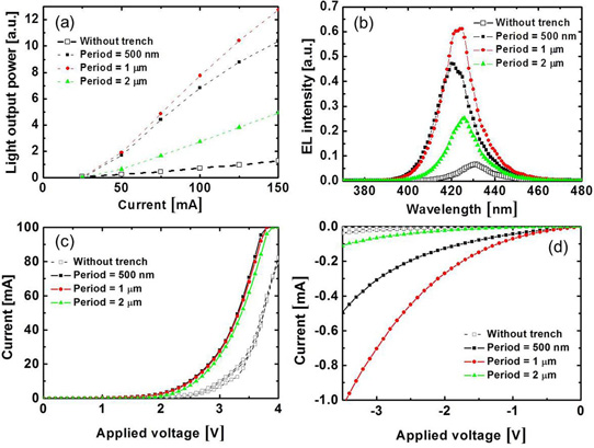
Figure 2: (a) Light output power of p-type trench structure using electron-beam lithography and conventional structure; (b) electroluminescence (EL); and (c) forward and (d) reverse current characteristics.
The researchers estimate that their devices without trenches emit about 5% of the light output power of commercial LEDs with similar active region area. Creating trenches by dry etch increases light output and blue-shifts the emission to shorter wavelengths (Figure 2).
The light output was greatest for 1μm period trenches. The researchers comment: "This is because the p-type trench structures also reduce the volume of the MQW while reducing the strain and the QCSE. Therefore, in order to maximize the light output power, it is important to optimize the ratio between the trench structure volume and the remaining MQW volume."
The wavelength shift was greatest with a 500nm period – from 431nm without trenches to 420nm. The effective bandgap was thus increased from 2.76eV to 2.85eV. This is attributed to strain relaxation.
The p-trenches increased forward current for a given voltage, but also increased leakage under reverse bias.
Wet etching of trenches also increased light output power, but not as dramatically. Further the technique was not as effective in relaxing strain, as evidenced by a minimal shift in emission wavelength. The current-voltage behavior was also less affected by the wet etch trenches.
http://dx.doi.org/10.1063/1.4973995
The author Mike Cooke is a freelance technology journalist who has worked in the semiconductor and advanced technology sectors since 1997.


