


- News
16 January 2017
Fully vertical and quasi-vertical gallium nitride pn diodes on silicon
Massachusetts Institute of Technology (MIT) in the USA has developed quasi-vertical and fully vertical pn gallium nitride diodes on silicon, claiming numbers of record performance characteristics [Yuhao Zhang et al, IEEE Electron Device Letters, published online 30 December 2016]. The researchers see possible application of the techniques to include vertical power transistors and advanced rectifiers, leading to competitive low-cost devices for 200-600V power switching.
Vertical devices offer improved breakdown voltage, current handling and thermal performance in a smaller footprint, compared with more conventional lateral GaN high-electron-mobility transistors (HEMTs), planar metal-oxide-semiconductor field-effect transistors (MOSFETs) and Schottky barrier diodes. However, most reports of vertical GaN devices use expensive gallium nitride substrates. The MIT researchers estimate silicon wafer costs at $0.08/cm2, which compares with ~$2.2/cm2 for 4-inch sapphire and ~$100/cm2 for 2-inch GaN substrates.
The III-nitride epitaxy consisted of metal-organic chemical vapor deposition (MOCVD) on 2-inch (111) silicon. The transition layers used aluminium gallium nitride (AlGaN) alloys. The semi-insulating GaN was achieved with iron doping. The low-electron-carrier-density n--GaN drift layer used carbon doping with propane precursor.
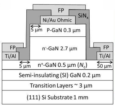
Figure 1: Quasi-vertical pn diode with passivation and field-plate (FP) structures.
The quasi-vertical diodes (Figure 1) used deep etch down to the n-GaN cathode layer for mesa isolation and silicon nitride passivation.
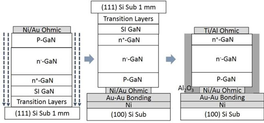
Figure 2: Fabrication sequence for fully vertical pn diode.
For the fully vertical structure (Figure 2), the epitaxial material was flipped and bonded to a (100) silicon substrate. Before bonding, the device mesa-isolation regions were defined by deep etching down to the (111) silicon growth substrate.
The compression bonding was carried out at 300°C for 20 minutes. A nickel layer protected the (100) silicon wafer during the sulfur hexafluoride (SF6) deep plasma etch used to remove the growth substrate. Further etching through the transition layers exposed the n+-GaN contact for subsequent formation of the ohmic contact. Atomic layer deposition (ALD) aluminium oxide (Al2O3) provided 20nm-thick passivation.
At a forward bias of 5.3V, the differential specific on-resistance was 0.8mΩ-cm2 for the quasi-vertical diodes and 1mΩ-cm2 for the fully vertical diodes. The current density was of the order of kA/cm2. "This high forward current level is comparable to state-of-the-art GaN-on-GaN vertical diodes," the researchers write. The slightly higher differential on-resistance for the fully vertical device is attributed to flow through the silicon substrate and etch-induced defects in the n+-GaN under the top ohmic contact.
The specific on-resistance of the fully vertical diode as a simple voltage/current ratio was 3mΩ-cm2 at 5.5V (so the current density (V/R) was 1.8kA/cm2). This is claimed as "the best report for all GaN-on-Si vertical diodes".
The breakdown voltage under reverse bias was more than 500V for both devices. The leakage at 300V reverse bias was around 5x10⁻³A/cm2, and still less than 10-2A/cm2 at 400V. These values are two orders of magnitude better than previous GaN-on-Si vertical diodes, according to the team. Further, the leakages are the lowest among all reported GaN vertical diodes on foreign substrates, lower than for lateral GaN diodes, and comparable with commercial SiC diodes, it is claimed.
The peak electric field was estimated to be 2.5-2.6MV/cm. Reference diodes without the carbon-doped n--GaN layer demonstrated lower breakdown voltage and increased reverse bias leakage. The researchers believe that reducing edge-type dislocations could increase the breakdown to 800V. Even higher values could be achieved with material able to sustain higher peak fields in the 2.8MV/cm-2.9MV/cm range.
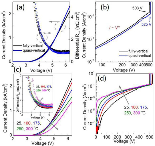
Figure 3: (a) Forward and (b) reverse characteristics of diodes, along with corresponding (c and d) temperature-dependent measurements.
The devices also performed well at increased temperatures up to 300°C with little degradation of on-resistance. The differential on-resistance at 300°C was as low as 1.35mΩ-cm2. Improved heat management could be provided by substrate thinning.
The devices also had reverse recovery times (~50ns, for switching from ~400A/cm2 to 200V reverse bias) "comparable to the best reports for GaN-on-GaN diodes". Another claimed record for GaN-on-Si vertical diodes is the Baliga figure of merit (BV2/Ron) of 0.32GW/cm2.
pn GaN diodes on silicon GaN MOCVD
https://doi.org/10.1109/LED.2016.2646669
The author Mike Cooke is a freelance technology journalist who has worked in the semiconductor and advanced technology sectors since 1997.


