


- News
14 February 2017
FBH's new CV measurement method offers more specific approach to UV LED device optimization
Aluminium gallium nitride (AlGaN)-based light-emitting diodes (LEDs) with ultraviolet (UV) emission at wavelengths of 250-320nm are promising devices for applications such as water purification, gas sensing, and UV curing. However, the lifetime of these UV LEDs is still limiting their applicability.
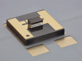 Figure 1: Typical image of flip-chip mounted UV LED on an AlN submount.
Within the Joint Lab GaN Optoelectronics of Ferdinand-Braun-Institut, Leibniz-Institut für Höchstfrequenztechnik (FBH) of Berlin, Germany and the Institute of Solid State Physics at Technische Universität Berlin (TU Berlin), UV-B and UV-C LEDs with emission wavelengths of 310nm and 265nm have been developed. To enhance the lifetime, deep knowledge about the physical mechanisms behind the stress-induced degradation is needed. The UV-B and UV-C LEDs were therefore exposed to accelerated aging for 200 hours at a constant current density of 140A/cm2 and different temperatures. It turned out that the reduction in the optical power is more pronounced and strongly temperature-dependent for UV-C LEDs compared with UV-B LEDs. To better understand this discrepancy, the LEDs were analyzed before and after stress by means of capacitance-voltage (CV) measurements.
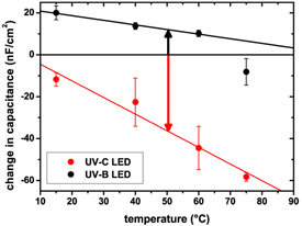 Figure 2: Change in measured device capacitance due to a 200hr constant current stress as a function of heat sink temperature during stress.
This method allows access to the widths of space charge regions (SCR) within the LEDs. Comparing the capacitances before and after stress reveals the impact of the temperature during stress (see Figure 2). While the capacitance gets smaller for the investigated UV-C LEDs (which can be attributed to an enlargement of the SCR), the capacitance of the UV-B LEDs increased for stress temperatures ≤60°C. This opposite behavior indicates that at least two different degradation mechanisms are prominent in these devices.
Further investigation of the UV-B LEDs showed that the capacitance increases mostly at the beginning of stress. This leads to the question of where exactly the changed SCR is located within the heterostructure. The researchers therefore developed a method for measuring the p-side of the stressed device alone. This allows the effects of the p-side to be separated from those of the pn-junction and the n-side of the heterostructure. The investigations show that the initial increase in capacitance can be attributed to changes in the p-side of the LED (see Figure 3). The stress is assumed to activate magnesium acceptors in the semiconductor.
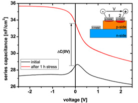 Figure 3: CV profiles of two p-contacts measured in series before (black) and after (red) stress of the LED-structure underneath one of these contacts.
The described method offers new possibilities for degradation studies in UV LEDs, say the researchers. In particular, the possibility of locating the changes in the LED structure should enable a more specific approach to device optimization.
The work was partially supported by the German Federal Ministry of Education and Research (BMBF) through the consortia project 'Advanced UV for Life' under contracts 03ZZ0105A and 03ZZ0105B. Further support was given by the Federal Ministry for Economic Affairs and Energy (BMWi) through the project 'UV-Berlin' under contract 03EFCBE067 as well as by the Deutsche Forschungsgemeinschaft within the Collaborative Research Center 'Semiconductor NanoPhotonics' (CRC 787).
http://ieeexplore.ieee.org/document/7774995


