


- News
15 February 2017
Gallium nitride on silicon on insulator metal-organic vapor phase epitaxy
Researchers based in Finland and Poland have compared gallium nitride (GaN) grown on bulk silicon with material grown on silicon-on-insulator (SOI) wafers [J. Lemettinen et al, Semiconductor Science and Technology, accepted manuscript online 13 January 2017].
Along with lower dislocation densities in GaN/SOI, the researchers from Aalto University in Finland, the Institute of Electronic Materials Technology in Poland and Okmetic Oyj in Finland found 400V higher breakdown in vertical through-wafer current testing. "These results show that the GaN-on-SOI platform is promising for power electronics applications," the team comments.
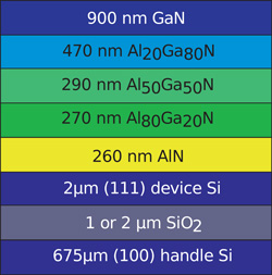 Figure 1: Schematic cross-sectional view of layer stack fabricated on SOI substrate.
Along with providing templates for power high-electron-mobility transistors (HEMTs) or light-emitting diodes (LEDs), the researchers suggest that the insulating buried oxide (BOX) layer of the SOI wafer could reduce losses and crosstalk in high-frequency applications.
Three different 6-inch substrates were compared: 1000μm-thick bulk silicon, and SOI wafers with 2μm silicon on 1μm- or 2μm-thick BOX layers. The silicon was oriented with the (111) surface suitable for GaN growth. The handles for the SOI wafers were 650μm (100) p-Si. Okmetic supplied the substrates.
Metal-organic vapor phase epitaxy (MOVPE) was performed using standard 1060°C step graded AlGaN layers to transition between the aluminium nitride (AlN) nucleation and GaN top layers (Figure 1). The 260nm AlN was grown at 980°C and 1085°C. The GaN layer was grown at 1040°C. Variations in the AlGaN buffer layers with 0.5x and 1.5x scaling were also implemented (see Table 1). The buffers were grown at 100mbar pressure, while the GaN was grown at 400mbar.
Table 1: Fabricated sample structures, with thicknesses in μm.
| Sample | A | B | C | D | E | F |
| Handle Si | 1000 | 675 | 675 | 675 | 675 | 675 |
| BOX | - | 1 | 1 | 2 | 2 | 2 |
| Device Si | - | 2 | 2 | 2 | 2 | 2 |
| AlN/AlGaN buffer | 1 | 1 | 1.5 | 0.5 | 1 | 1.5 |
| GaN | 1 | 1 | 1 | 1 | 1 | 1 |
The researchers comment: "The higher growth pressure increases the crystalline quality of GaN while material grown at 100mbar pressure has a higher carbon concentration and forms a semi-insulating layer. This type of semi-insulating layer is typically used for device insulation, for example, in GaN HEMT."
Defects and strain of the resulting materials were studied using x-ray analysis and selective etching. Although the x-ray diffraction peaks of GaN/SOI were broader, the etched defects were about half that for material grown on bulk Si. However, the etching results were in line with detailed x-ray studies that differentiated dislocation types in terms of ratios and density (see Table 2). Deeper studies of strain conditions resulted from synchrotron x-ray topography carried out at the TOPO-TOMO beamline of the ANKA (Angströmquelle Karlsruhe) facility in Germany.
Table 2.
| Sample | A | B | C | D | E | F |
| Total (1010/cm2) | 1.93 | 1.02 | 0.82 | 0.914 | 0.73 | 0.833 |
| Edge (1010/cm2) | 1.93 | 0.73 | ||||
| Screw and mixed (107/cm2) | 0.81 | 1.34 |
Among their discoveries, the researchers found that a thicker BOX layer allowed them to reduce the buffer thickness while maintaining GaN quality. They comment: "The thinner buffer reduces the growth time by 1 hour, and thus reduces the total process cost. In addition, our results indicate that varying the SOI device Si layer thickness could lead to even better crystalline quality."
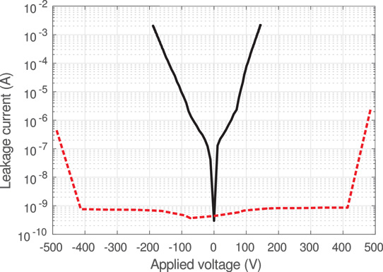
Figure 2: Vertical through-substrate leakage current of epitaxial layers of sample A grown on bulk Si (black, solid) and sample E grown on SOI (red, dashed) substrate.
Vertical through-substrate leakage current measurement found that the BOX layer significantly improved breakdown characteristics – "the onset of breakdown is delayed by approximately 400V," according to the researchers (Figure 2). "The vertical through-substrate current of sample A is approximately the same at 80V bias than sample E current at 480V bias," they add. The contacts for the measurements were aligned 1mmx1mm pads of titanium and gold on the top and bottom of the wafer.
https://doi.org/10.1088/1361-6641/aa5942
The author Mike Cooke is a freelance technology journalist who has worked in the semiconductor and advanced technology sectors since 1997.


