


- News
13 December 2017
Monolithic III-nitride on silicon photonics for Internet of Things
Nanjing University of Posts and Telecommunications and Zhengzhou University in China have been developing III-nitride technology for visible light communication (VLC) on a monolithic silicon platform [Xumin Gao et al, Optics Letters, vol42, p4853, 2017].
In particular, the team created a system of a light-emitting diode transmitter and photodiode receiver linked by an indium gallium nitride (InGaN) waveguide in aluminium gallium nitride (AlGaN) cladding. Transmission at up to 200Mbits per second (Mb/s) was demonstrated for both in-plane and out-of-plane set ups. The in-plane transmission to an on-chip receiver could be used in practice as a power monitor.
The team sees particular benefit arising for ‘Internet of Things’ applications, along with integrated biomedical analysis systems and monolithic photonic circuits. “From a mass-production point of view, the III-nitride-on-silicon platform offers a feasible approach that is compatible with Si-fab for wafer-level fabrication,” the researchers add.
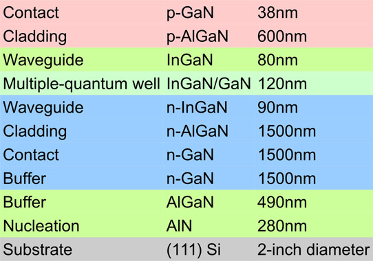
Figure 1: Epitaxial structure.
The device fabrication was performed on 2-inch III-nitride on silicon substrates produced by metal-organic chemical vapor deposition (MOCVD) – see Figure 1. The further processing (Figure 2) consisted of 590nm mesa isolation etch, the formation of an annealed nickel/gold p-contact, etching to the n-contact layer, plasma-enhanced chemical vapor deposition (PECVD) of 200nm silicon dioxide isolation, buffered oxide etch of electrode regions, and titanium/platinum/gold metalization. The transmitter and receiver were isolated from each other by the removal of the p-GaN layer from the top of the waveguide.
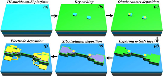
Figure 2: Fabrication processes of multi-component system on III-nitride-on-Si platform.
The photonic circuit consisted of an 8μm-wide, 200μm-long InGaN waveguide connecting a transmitter and receiver. The transmitter was found to emit radiation with a wavelength around 452nm. The transmitter diode turn-on voltage was around 2.5V. The capacitance of the device was around 2.33pF at 500kHz. A lower capacitance would improve the modulation capability.
The photocurrent through the receiver diode was found to follow the increased emission from the transmitter with increased current injection. The response to an on-off keying modulation, pseudo-random binary sequence (PRBS) data stream gave ‘open eye’ diagrams with rates up to 200Mb/s, the limit of the measurement system.
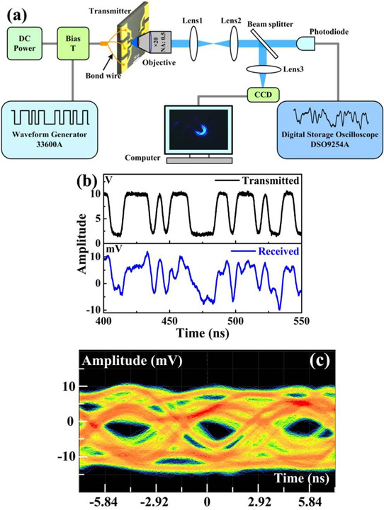
Figure 3: (a) Schematic out-of-plane visual light communication. (b) Transmitted and received PRBS data at 200Mb/s transmission rate. (c) Eye diagrams measured at 200Mb/s.
Out-of-plane light was collected by 20x objective lens with 0.5 numerical aperture (NA) and transmitted through a confocal system to a photodiode (Figure 3). Under 200Mb/s data streams the system again gave open-eye diagrams.
InGaN AlGaN Silicon photonics Internet of Things Silicon substrates MOCVD
https://doi.org/10.1364/OL.42.004853
The author Mike Cooke is a freelance technology journalist who has worked in the semiconductor and advanced technology sectors since 1997.


