


- News
11 December 2017
Fins boost prototype vertical GaN transistor to 1200V, sufficient for electric vehicles
© Semiconductor Today Magazine / Juno Publishing
Commercial gallium nitride (GaN) power devices cannot handle voltages above about 600V, limiting their use to household electronics. But at the Institute of Electrical and Electronics Engineers’ International Electron Devices Meeting (IEDM), researchers from Massachusetts Institute of Technology (MIT), epiwafer and substrate maker IQE plc, Columbia University, IBM and the Singapore-MIT Alliance for Research and Technology presented a new design that, in tests, enabled gallium nitride (GaN) power devices to handle voltages of 1200V.
That is already enough capacity for use in electric vehicles, but the device is a first prototype manufactured in an academic lab. But, since the new device uses a fundamentally different design from existing GaN power electronics, the researchers believe that further work can boost the voltage to 3300-5000V, bringing the efficiencies of GaN to the power electronics in the electrical grid itself.
“All the devices that are commercially available are what are called lateral devices,” says the paper’s senior author Tomás Palacios, who is an MIT professor of electrical engineering and computer science, a member of the Microsystems Technology Laboratories. “So the entire device is fabricated on the top surface of the gallium nitride wafer, which is good for low-power applications like the laptop charger. But for medium- and high-power applications, vertical devices are much better,” he adds. “These are devices where the current, instead of flowing through the surface of the semiconductor, flows through the wafer, across the semiconductor. Vertical devices are much better in terms of how much voltage they can manage and how much current they control.”
Firstly, current flows into one surface of a vertical device and out the other, so there’s more space in which to attach input and output wires, enabling higher current loads.
Secondly, when you have lateral devices, all the current flows through a very narrow slab of material close to the surface. “We are talking about a slab of material that could be just 50nm in thickness,” Palacios says. “So all the current goes through there, and all the heat is being generated in that very narrow region, so it gets really, really, really hot. In a vertical device, the current flows through the entire wafer, so the heat dissipation is much more uniform.”
Narrowing the field
Although their advantages are well-known, vertical devices have been difficult to fabricate in gallium nitride. For transistor switching to be efficient, the current flowing through the semiconductor needs to be confined to a relatively small area, where the gate’s electric field can exert an influence on it. In the past, researchers had attempted to build vertical transistors by embedding physical barriers in the GaN to direct current into a channel beneath the gate.
But the barriers are built from a temperamental material that’s costly and difficult to produce, and integrating it with the surrounding GaN in a way that doesn’t disrupt the transistor’s electronic properties has also proven challenging.
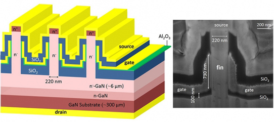
Picture: In the vertical GaN transistors, the narrowness of the fins ensures that the gate electrode will be able to switch the transistor on and off.
Palacios and his collaborators have adopted a simple but effective alternative. Rather than using an internal barrier to route current into a narrow region of a larger device, they simply use a narrower device. Their vertical GaN transistors have blade-like protrusions (fins) on top. On both sides of each fin are electrical contacts that together act as a gate. Current enters the transistor through another contact, on top of the fin, and exits through the bottom of the device. The narrowness of the fin ensures that the gate electrode will be able to switch the transistor on and off.
The idea was to say, “Instead of confining the current by having multiple materials in the same wafer, let’s confine it geometrically by removing the material from those regions where we don’t want the current to flow,’” Palacios says. “Instead of doing the complicated zigzag path for the current in conventional vertical transistors, let’s change the geometry of the transistor completely.”
https://tlo.mit.edu/technologies/new-structures-gan-vertical-transistors


