


- News
1 December 2017
Reducing bow of indium gallium phosphide on silicon wafers
Researchers based in Singapore and the USA have been working to control the wafer bow of indium gallium phosphide (InGaP) epitaxial layers on 200mm silicon (Si) wafers [Bing Wang et al, Semicond. Sci. Technol., vol32, p125013, 2017].
Wafer bow is caused by stress arising mainly from mismatches of coefficients of thermal expansion between InGaP, or other III-V compound semiconductors, and Si. The bow (more than 200μm in one recent report of gallium arsenide on 300mm Si wafer) is introduced when the material cools after high-temperature epitaxial deposition. Bowing adversely affects wafer-scale processing, particularly for large-diameter substrates. Wafer-scale equipment typically restricts the permitted bow to less than 50μm.
The team from Singapore-MIT Alliance for Research and Technology, Nanyang Technological University in Singapore, and Massachusetts Institute of Technology in the USA used strain engineering to reduce bow in InGaP templates grown on high-quality germanium (Ge) buffers on silicon.
The 200mm (8”) silicon substrate was offcut 6º toward the nearest {111} plane. Epitaxy was by metal-organic chemical vapor deposition (MOCVD). The germanium on silicon template layer was prepared separately in a two-step low/high-temperature process, using germane (GeH4) precursor. Plan-view transmission electron microscopy (PVTEM) and etch pit density (EPD) analysis gave an estimate of dislocation density of the order 3x10⁷/cm2.
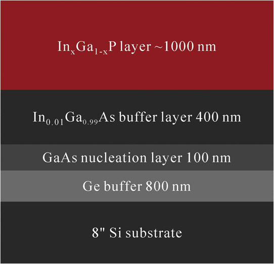
Figure 1: Epitaxial layer structure of three InGaP/Si wafers.
The MOCVD reactor was thoroughly cleaned to remove Ge residues before III-V epitaxy (Figure 1), avoiding uncontrollable n-type doping. The group-III metal-organic precursors were trimethyl-gallium and trimethyl-indium. The group-V arsenic (As) and phosphorus (P) components were delivered by arsine (AsH3) and phosphine (PH3), respectively. Hydrogen was the carrier gas.
The 1%-indium-content InGaAs formed the main part of the buffer since its lattice mismatch with Ge was smaller than that of pure GaAs. Three InGaP compositions were produced: lattice-matched with 49% indium content, along with non-matched 52% and 54% samples. The MOCVD temperature was 630ºC, with less than 10ºC variation across the wafer.
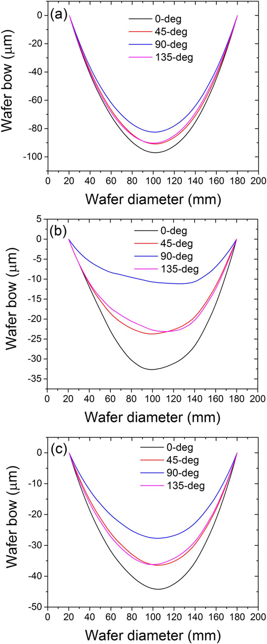
Figure 2: Wafer bow of InGaP wafers: x = 0.49 (a), x = 0.54 (b), and x = 0.52 (c). Wafer notch orientation (1–10) is 0º, and (110) direction is 90º.
Atomic force microscopy showed increasing roughness as the InGaP became more mismatched – 1.68nm root-mean-square for In0.49Ga0.51P, 2.08nm for In0.52Ga0.48P, and 2.34nm for In0.54Ga0.46P. The roughness of the GaAs buffer was 0.8nm. The wafers exhibited anisotropic concave bows of up to 97μm (Figure 2). The bow was greatest for the In0.49Ga0.51P, decreasing with increase in indium content.
Table 1: Summary of InGaP sample compositions, wafer bow, strain, relaxation, and TDDs.
|
Sample
InxGa1−xP |
Wafer bow | Strain | Relaxation | EPD (x107/cm2) |
PVTEM (x107/cm2) |
| x = 0.49 | −82.5μm (110) −97μm (1–10) |
0.251% 0.222% |
−37% 29% |
1.5 | 3.1 |
| x = 0.54 | −11μm (110) −32.7μm (1–10) |
−0.054% −0.041% |
17.5% 25.5% |
1.6 | 2.8 |
| x = 0.52 | −27.7μm (110) −44.2μm (1–10) |
0.012% −0.003% |
−0.9% 1.5% |
1.7 | 1.9 |
X-ray reciprocal space map analysis was used to assess strain in the resulting wafers (Table 1). The lattice-matched In0.49Ga0.51P wafer was observed to have a tensile strain and the In0.54Ga0.46P sample was under compression. The middle In0.52Ga0.48P material was slightly tensile strained (0.01%) along the (110) direction and compressed (-0.003%) along the (1-10) direction.
The researchers point out that dislocation mobility is anisotropic, commenting “anisotropic strain and relaxation correlate with the anisotropic wafer bow very clearly.” They add: “compensation of the thermal stress by the lattice-mismatch strain decreases the wafer bow.”
The threading dislocation density (TDD) of the InGaP layers was about the same at 1.6x10⁷/cm2, according to EPD analysis. PVTEM gave an estimate of 3.1x10⁷/cm2 for the In0.49Ga0.51P wafer.
The researchers comment: “Based on these observations, we can conclude that the TDDs of the InGaP wafers are not affected by the lattice mismatch. Our Ge buffers have similar TDD of 3x10⁷/cm2. The hetero-epitaxy of GaAs buffers and InGaP films did not increase the TDD, which indicates very good epitaxy quality.” The team believes the technique can be applied to other III-V systems on silicon.
Wafer bow InGaP Si wafers MOCVD
https://doi.org/10.1088/1361-6641/aa952e
The author Mike Cooke is a freelance technology journalist who has worked in the semiconductor and advanced technology sectors since 1997.


