


- News
20 December 2017
Deep ultraviolet photonic crystal of aluminium gallium nitride nanowires
Researchers based in the USA and Canada have used selective area epitaxy to develop arrays of aluminium gallium nitride (AlGaN) nanowires for deep ultraviolet (DUV) light emission [Xianhe Liu et al, Optics Express, vol25, p30494, 2017]. The team from University of Michigan in the USA and McGill University and McMaster University in Canada hope that their work will lead to more efficient DUV photonics. At present, AlGaN-based light-emitting diodes achieve external quantum efficiencies much less than 10%.
Applications of UV-C – less than 280nm wavelength – include water purification, disinfection, surface treatment, and medical diagnostics. AlGaN materials provide photon emissions in the energy range 3.4eV for pure GaN up to 6.2eV, corresponding respectively to wavelengths of 365nm and 200nm.
The researchers hope that regular ‘photonic crystal’ structures of AlGaN nanowires will boost efficiency, overcoming the unfortunate tendency of the light in high-Al-content AlGaN to be emitted with transverse magnetic (TM) polarization leading to in-plane propagation, inhibiting photon extraction. Theoretical studies suggest that light extraction efficiency can be increased to more than 70% with AlGaN nanowire photonic crystals.
Forming photonic crystals requires precise placement of nanowires through some form of selective-area epitaxy. The team comments: “To date, however, selective area epitaxy has not been successfully applied to Al-rich AlGaN nanowires, and there has been no demonstration of AlGaN nanowires emitting in the UV-C band by selective area epitaxy, which is partly limited by the high temperature (often >1000°C) required for AlN epitaxy and the lack of a suitable growth mask.”
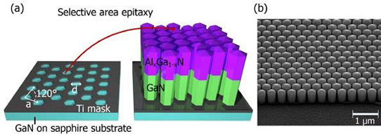
Figure 1: (a) Left: nanoscale aperture arrays defined by electron-beam lithography on 10nm thick titanium mask on c-plane GaN-on-sapphire substrate. Right: schematic of selective area epitaxy of GaN/AlGaN nanowires on patterned substrate. (b) Scanning electron microscope image of resulting GaN/AlGaN nanowire arrays.
Selective-area growth was performed on c-plane GaN-on-sapphire templates in a molecular beam epitaxy (MBE) system made by Veeco. A 10nm titanium mask was used with hexagonal apertures in a triangular lattice formation (Figure 1). After nitriding the mask, GaN nanowire templates were grown at 995°C, according to sensors on the back-side of the substrate. The AlGaN part of the nanowire was grown at temperatures in the range 935-1025°C. The shell of the nanowires was Al-rich, a feature expected to reduce non-radiative surface recombination of charge carriers.
By varying the AlGaN composition, a range of wavelengths – 210-327nm – was obtained in photoluminescence (PL) measurements.
LEDs with 280nm wavelength were fabricated from nanowires with 300nm of n-GaN, 80nm of n-Al{0.64Ga0.36N, 30nm of undoped Al0.48Ga0.52N, and 60nm of p-Al{0.64Ga0.36N . The undoped region constituted the active light-emitting part of the device. The growth used a substrate temperature of 1025°C. The axial growth rate was ~150nm/hour. The nanowires also grew sideways, filling the air gaps of the lattice at a rate of ~20nm/hour.
The structure had a PL wavelength of 283nm and a linewidth of 11nm. The narrow width of the peaks indicates the improved uniformity over spontaneously grown nanowires. At higher excitation powers, the p-/n-AlGaN cladding layers contribute a peak around 255nm. Comparing low- and high-temperature PL responses suggested an internal quantum efficiency of 45% (or 49% at higher excitation power) at room temperature.
The LED fabrication consisted of spin-coating polyimide, etching back to reveal the tops of the nanowires, oxide removal with hydrochloric acid, and deposition, annealing and patterning of metal contacts – nickel/gold on the p-GaN and titanium/gold on the n-GaN layers. The p-contact metal was patterned into a grid.
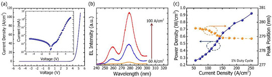
Figure 2: (a) Current-voltage characteristics of AlGaN nanowire LED. Inset: same characteristics in semi-log scale. (b) Electroluminescence spectra of AlGaN nanowire LEDs measured under different injection currents. (c) Power density and peak position as a function of current density measured at room temperature under pulsed biasing condition.
A 50μmx50μm device had a turn-on voltage of 4.4V, and at 5V the current density was 100A/cm2 (Figure 2). This performance is better than previously reported AlGaN quantum well LEDs operating at similar wavelengths, according to the team.
The peak wavelength was at 279nm with a very small blue-shift with increasing current – moving from 279.6nm at 50A/cm2 to 278.9nm at 252A/cm2. Some carrier overflow is evident in a weak emission peak at 260nm, which is attributed to recombination in the cladding (most likely on the p-side). The measurements avoided self-heating effects by pulsed operation.
The researchers estimate the output power at 0.93W/cm2 with 252A/cm2 injection. That would give a raw efficiency, not correcting for contact/series resistance, of the order 0.07% (0.93W/252A/5V), so much work needs to be done to get to 10% efficiencies.
The researchers comment: “The output power can be significantly increased by optimizing the nanowire size and spacing to achieve enhanced light extraction for TM polarized emission. Moreover, the device performance can be further improved by utilizing the scheme of tunnel junction to significantly enhance the hole injection and transport.”
AlGaN AlGaN Nanowires DUV LEDs
https://doi.org/10.1364/OE.25.030494
The author Mike Cooke is a freelance technology journalist who has worked in the semiconductor and advanced technology sectors since 1997.


