


- News
13 December 2017
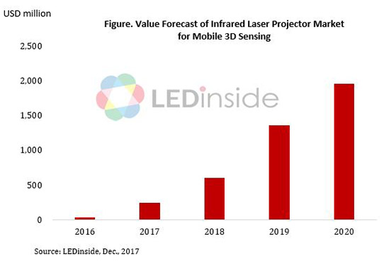
Infrared laser projector market for mobile 3D sensing to grow from $246m in 2017 to $1.953bn in 2020
© Semiconductor Today Magazine / Juno Publishing
As many smartphone companies have been developing 3D sensing embedded devices since Apple launched the iPhone X featuring a 3D sensor, the infrared laser projector market for mobile 3D sensing will reach US$246m in 2017 then grow to about US$1.953bn in 2020, forecasts LEDinside (a division of TrendForce) in its ‘2018 Infrared Sensing Application Market Report’.
An infrared laser projector has three major components, including a vertical-cavity surface-emitting laser (VCSEL) or edge-emitting laser (EEL), wafer-level optics (WLO) and diffractive optical elements (DOE). The current cost of an infrared laser projector is about US$3.5-6, but this is expected to decrease as the technology advances and supply chain strategy improves, boosting market demand as a result, says LEDinside research manager Joanne Wu.
Existing solutions for mobile 3D sensing include structured light and time of flight (ToF). The iPhone X uses structured light and its dot projector produces more than 30,000 dots of infrared lights on the face. Then the infrared camera receives the light reflected back from the face to create a 3D facial landscape.
In addition to 3D face sensing, branded smartphone makers also actively integrate 3D sensing with augmented reality (AR). LEDinside therefore forecasts that 3D sensor may be incorporated either in the front camera or in the rear camera. Manufacturers are expected to use ToF for the rear camera, as ToF can scan a larger area with better performance in computing and data processing. Moreover, ToF corresponds to the patent strategies of 3D sensing technology providers.
Regarding the supply chain for 3D sensing, LEDinside notes that algorithms, the emission pattern and patents will be the three key elements for 3D sensing development in the future.
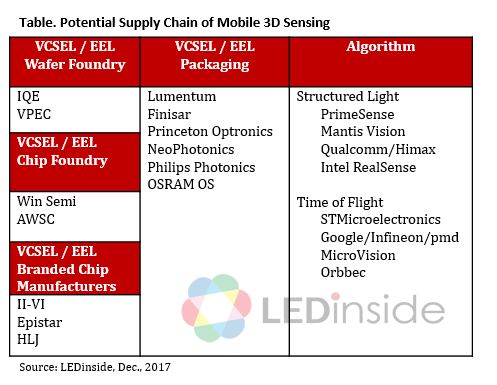
VCSEL/EEL wafer and chip foundries (e.g. IQE, VPEC, WIN Semiconductor, II-VI Inc, Epistar, HLJ, AWSC) have increased their production capacity. Major VCSEL/EEL packaging companies include Lumentum, Finisar, Princeton Optronics, NeoPhotonics, Philips Photonics, and Osram Opto Semiconductors.
In addition to Apple, Samsung and ASUS, Chinese smartphone brands such as Xiaomi, Lenovo, Huawei and OPPO all plan to release new phones with 3D sensing,
Smartphone brands are now deploying in the market and seeking cooperation within the supply chain. However, obstacles still remain for the future development of the 3D sensing market, cautions LEDinside, including obtaining patents, developing third-party application, and increasing the performance-price ratio.


