


- News
1 December 2017
Removing sapphire substrate from light-emitting diodes without cracking
Ferdinand-Braun-Institut and Technische Universität Berlin in Germany have developed a fabrication process for deep ultraviolet (DUV) light-emitting diodes (LEDs) that allows laser lift-off (LLO) separation of the sapphire growth substrate without chipping or cracking damage of the device [H K Cho et al, Semicond. Sci. Technol., vol32, p12LT01, 2017]. The LLO was performed at the chip level. The researchers developed a titanium/gold leveling layer that provided support for the fragile epitaxial film during the thermal shock of the LLO and subsequent processes.
The researchers see DUV LEDs as having potential for sterilization, water purification, medical diagnostics, phototherapy and UV curing. Removal of the sapphire substrate, and subsequent surface texturing, is seen as a route to increasing light extraction efficiency, boosting overall external quantum efficiency from the single-digit percentages presently achieved in the DUV region.
The process also allows the use of thin films of planar solder instead of gold stud bumps for mounting, which should improve thermal management in applications. “To the best of our knowledge, LLO of the sapphire substrate from DUV LEDs flip-chip mounted via solder has not yet been reported,” the team writes.
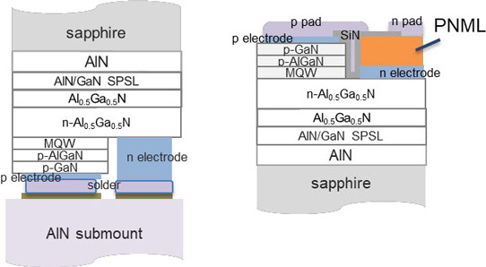
Figure 1: Schematic of AlGaN-based heterostructure and DUV LED chip on AlN submount (left) and chip structure with PNML (right).
Metal-organic chemical vapor deposition (MOCVD) on (0001) sapphire resulted in a DUV LED structure (Figure 1) with a 900nm AlN buffer, 200nm 80x(AlN/GaN) short-period superlattice (SPSL) with 0.65 Al mole fraction average, 600nm Al0.5Ga0.5N, 4.2μm silicon-doped n-Al0.5Ga0.5N contact, 3x(AlGaN/AlGaN) multiple quantum well (MQW) active region, p-AlGaN electron blocking layer, p-AlGaN/AlGaN superlattice, and a p-GaN contact.
Fabrication began with exposure of the n-contact layer with reactive ion etch and formation of an ohmic vanadium/aluminium/nickel/gold contact with electron-beam evaporation and 725°C annealing. The p-contact was palladium annealed at 530°C. Silicon nitride passivation was applied by plasma-enhanced chemical vapor deposition (PECVD). The chips were completed with soldering pads and dicing into 1mmx0.6mm dies. The active area was 0.07mm2. The chips were bonded to AlN submounts with gold-tin solder.
Before mounting, some of the chips had an added p and n metal leveling layer (PNML) deposited on the n-electrode, consisting of 30nm of titanium and 70nm of gold. The researchers believe that the PNML in particular fills the region between the p- and n-electrodes, giving a flat surface topography.
A 248nm-wavelength krypton-fluoride excimer laser was used to remove the sapphire substrate. The beam spot was larger than the chip, at 2mmx2mm. “The sapphire substrate lifted off spontaneously by itself after LLO without the need of activation by subsequent steps,” the team reports. Residue from the process was removed with hydrochloric acid solution.
Without the PNML, the LLO process tended to result in chipping and cracking, mostly in the region between the p- and n-electrodes. The researchers explain: “This area can be easily damaged by the physical shock during LLO because it is free-standing without bonding to the submount. The thin metal layer of the n-electrode and the SiNx passivation layer on top are not sufficient to stabilize the epi layer in this area. The PNML fills the region between the p-pad and the n-pad, where it is thought to stabilize the fragile epitaxial structure.”
With the PNML, the team reports, “the device had no mechanical damage after LLO, i.e. the sapphire substrate was successfully removed without crack formation in the epitaxial layers or material chipping.”
Scanning electron microscope analysis of the LED surfaces showed that the LLO caused separation in the undoped Al0.5Ga0.5N layer, so that the AlN buffer and AlN/GaN SPSL layers were also removed with the sapphire.
Without the PNML, cracking was observed to be generated by the thermal shock of the LLO and propagated by the hydrochloric acid clean.
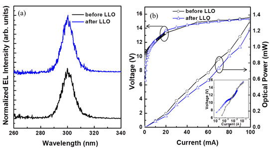
Figure 2: Performance of flip-chip-mounted DUV LEDs before and after LLO: Normalized emission spectra at a current of 20mA (a) and light output-current-voltage (L-I-V) characteristics (b).
The performance of the LEDs with PNML was not substantially affected by the LLO process (Figure 2), although there was a slight increase in leakage at low voltages.
DUV LEDs LLO Sapphire substrate GaN AlGaN
https://doi.org/10.1088/1361-6641/aa9402
The author Mike Cooke is a freelance technology journalist who has worked in the semiconductor and advanced technology sectors since 1997.


