


- News
16 August 2017
Indium gallium arsenide phosphide quantum wells on silicon on insulator
University of California Santa Barbara (UCSB) in the USA has developed direct growth of indium gallium arsenide phosphide (InGaAsP) multiple quantum well (MQW) nanowires on silicon-on-insulator (SOI) substrates [Ludovico Megalini et al, Appl. Phys. Lett., vol111, p032105, 2017]. The target emission wavelength of the MQWs was 1550nm infrared, as favored for fiber-optic communication applications. The team looks forward to “integration of InP-based nanoridges in the SOI platform for new classes of ultra-compact, low-power, nano-electronic, and photonic devices for future tele- and data-communications applications.”
SOI also has superior optical confinement properties compared to bulk silicon (Si): 13.4% confinement for SOI compared with 1.2% for Si, according to InGaAsP nanowire simulations by the UCSB research team. Both Si and SOI have been used as the basis for photonics platforms, with patterning of waveguides and other optical elements in advanced stages of development. The component lacking in this work is light-emitting and laser-emitting devices.
The SOI substrate used by UCSB had a 500nm lightly doped p-type Si layer on 1μm buried silicon dioxide. A 500nm plasma-enhanced chemical vapor deposition (PECVD) silicon dioxide layer was used as a mask patterned with 3mm-long, 200nm-wide, 800nm-pitch stripes along the [110] direction. The wafer was then diced into 2cmx2cm pieces.
The silicon device layer was etched with dilute potassium hydroxide at 70°C to give v-grooves with {111} surfaces. A small undercut at the interface between the mask and device layer was found to be useful for trapping defects – in particular, stacking faults – in the subsequent InGaAsP growth by metal-organic chemical vapor deposition (MOCVD).
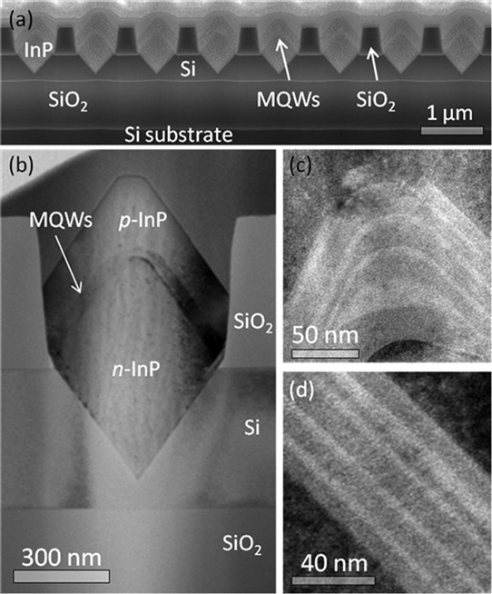
Figure 1: (a) Focused ion-beam scanning electron microscope (FIB-SEM) cross-section images of InP nanowires, showing regular morphology. (b) Bright-field transmission electron microscope (BF-TEM) image of single nanowire with good symmetry. (c and d) BF-TEM images of QWs and barrier layers in (c) (001) surface and (d) {11-1B} facet. Dark colored layer is barrier, light colored is quantum well.
The III-V layers consisted of 20nm of GaAs nucleation in two temperature steps of 410°C and 430°C, 430°C InP nucleation, continued InP growth at 550°C and 600°C, and finally 650°C growth of InGaAsP MQWs and 400nm InP cap (Figure 1). The InP nanowires were ~1.3μm thick with good height uniformity over a wide area, according to the researchers.
Photoluminescence experiments found a peak at 1555.7nm with 135nm full width at half maximum (FWHM), attributed to the MQW structures. The pump power was 20.5W/cm2. Lower pump powers gave a broader peak (Figure 2). This is attributed to saturation effects where the impact from defects becomes less significant at high excitation intensity.
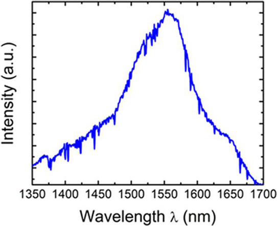
Figure 2: Photoluminescence spectrum showing emission at 1567nm from MQW structure inside InP nanowires grown on v-groove patterned SOI.
The MQW layers were also non-uniform, leading to peak shifts and broadening as the excitation spot position varied over the sample. Inhomogeneous spectrum broadening could inhibit gain in laser devices. The researchers believe more uniform QWs could be achieved with careful adjustment of growth time and position within the nanowire.
InGaAsP MQW nanowires SOI substrates PECVD MOCVD
http://dx.doi.org/10.1063/1.4994318
The author Mike Cooke is a freelance technology journalist who has worked in the semiconductor and advanced technology sectors since 1997.


