


- News
1 August 2017
ALLOS challenges conventional beliefs of GaN-on-Si
In the presentation ‘Low vertical leakage current of 0.07µm/mm2 at 600V without intentional doping for 7µm-thick GaN-on-Si’ at the 12th International Conference on Nitride Semiconductors (ICNS-12) in Strasbourg, France (24-28 July), Dr Atsushi Nishikawa, co-founder & chief technology officer of technology engineering & licensing firm ALLOS Semiconductors GmbH of Dresden, Germany, discussed three common beliefs about gallium nitride on silicon (GaN-on-Si): First, that the usage of intentional carbon doping would be inevitable, second that using interlayers in the buffer would be a source of leakage, and third that the choice of the right reactor hardware would be decisive for achieving good results. However, with the experimental evidence presented, Nishikawa the validity of these three widespread beliefs.
1. Developers of GaN-on-Si epiwafers are suffering from the fact that crystal impurities from the growth process cause the isolation of GaN to be far below its theoretically possible values. To overcome these deficiencies, GaN-on-Si epiwafer makers usually apply carbon doping to achieve the required isolation. Unfortunately, conventional methods of carbon and other doping have negative side-effects. In contrast, says Nishikawa, ALLOS’ results prove that, by focusing on superior crystal quality and thick GaN layers, the required low leakage currents can be achieved without any intentional carbon or other doping. This not only avoids the negative side-effects of doping but also widens the process window for further optimization of numerous manufacturing and electrical properties, he adds.
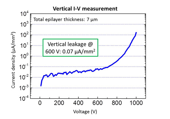
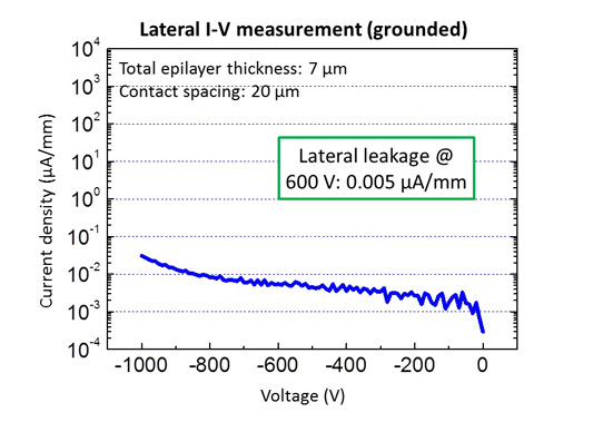
2. Nishikawa also presented experimental evidence that, rather than that interlayers being a source of leakage, in fact the opposite is true: Carefully controlled interlayer growth conditions and positioning of the interlayers can improve isolation by more than one order of magnitude, says Nishikawa. In combination, these techniques allow ALLOS to achieve very low vertical and lateral leakage currents of only 0.07µA/mm2 and 0.005µA/mm, respectively, at 600V. This is based on 7µm-thick GaN with very high crystal quality of 316 arcsec for (002) and 413 arcsec for (002) XRD (x-ray diffraction). Available on epiwafers of both 150mm and 200mm diameter with SEMI-standard thicknesses, ALLOS says that its technology is designed for manufacturability, is suitable for standard silicon lines, and has a controlled minimum bow and no cracks.
3. Regarding the belief that the choice of the right reactor hardware is decisive, Nishikawa acknowledges that, of course, good hardware matters but it is far from the dominant factor. ALLOS says that it can apply its structure and growth methods on several hardware platforms, as demonstrated by a comparison of results from two leading models of multi-wafer metal-organic chemical vapor deposition (MOCVD) reactor. On both reactors, similar material and electrical properties have been achieved, Nishikawa notes.
ALLOS' doping-free 600V HEMT epi technology running on both Aixtron G5 and Veeco K465i at customer
ALLOS transfers GaN-on-Si power semiconductor epi technology to customer
Transfer of ALLOS' 150 and 200mm GaN-on-Si epi technology to Epistar concluded in under 6 months


