


- News
10 April 2017
Fluorinated graphene passivation for aluminium gallium nitride transistors
Shanghai Institute of Microsystem and Information Technology and Shanghai Normal University in China have used fluorinated graphene (FG) to improve the performance of aluminium gallium nitride (AlGaN) metal-insulator-semiconductor high-electron-mobility transistors (MIS-HEMTs) [Lingyan Shen et al, IEEE Electron Device Letters, published online 15 March 2017]. The FG was inserted as passivation between the epitaxial semiconductor and the gate-insulator dielectric. The researchers claim that their work is the first use of FG for passivation of AlGaN/GaN HEMTs.
The performance was improved both in terms of DC testing but also under pulsed conditions, where current collapse is a continuing problem for III-nitride transistors. III-nitride devices are being developed for power and microwave applications.
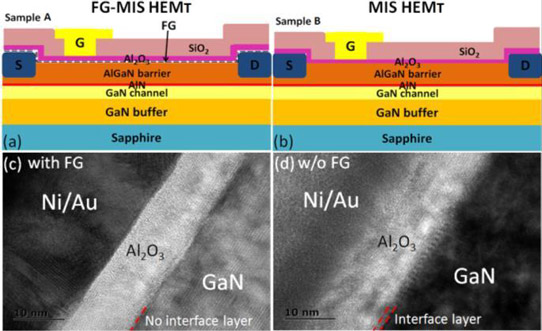
Figure 1: Schematic cross sections of (a) FG-MIS HEMT and (b) traditional MIS HEMT. HRTEM image in gate region of (c) FG-MIS HEMT and (d) traditional MIS HEMT.
The HEMT material was grown on sapphire with a layer sequence of 3.9μm carbon-doped GaN buffer, 300nm GaN channel, 1nm AlN spacer, 20nm AlGaN barrier, and 2nm GaN cap.
Device fabrication consisted of 400nm mesa etch, annealed titanium/aluminium/nickel/gold ohmic contacts, graphene transfer and fluoridation, 14nm atomic layer deposition (ALD) aluminium oxide, 200nm plasma-enhanced chemical vapor deposition (PECVD) silicon dioxide, and annealed nickel/gold gate formation on the aluminium oxide dielectric.
The graphene was grown by chemical vapor deposition (CVD) on copper foil. The graphene was then separated by electrochemical delamination and transferred to the HEMT. Fluoridation was achieved by exposure to sulfur hexafluoride plasma.
The HEMT parameters were 3μm gate length, 15μm gate-to-drain spacing, and 3μm gate-to-source spacing.
The fluorinated graphene increased the peak transconductance by 14%, compared with a conventional MIS-HEMT. The threshold voltage of the FG devices was also 0.6V more positive (see Table 1). However, the threshold was still negative, meaning that at 0V gate potential the device was ‘on’ - i.e. ‘normally-on’. Another improvement in the FG device was two-orders reduced leakage current in the ‘of’ state (as low as 10-8mA/mm).
Table 1: Extracted parameters from DC characteristics.
| Parameter | Unit | FG-MIS | MIS |
| Threshold | V | -6.7 | -7.3 |
| Peak transconductance | mS/mm | 44.6 | 39.0 |
| On-resistance | Ω-mm | 7.40 | 9.44 |
| Saturation drain current | mA/mm | 618 | 460 |
| Off current leakage | mA/mm | ~10-8 | ~10-6 |
| Gate leakage | mA/mm | ~10-6 | ~10-4 |
The researchers attribute the improved performance to a clear and sharp interface between the GaN cap and aluminium oxide gate dielectric in the FG MIS-HEMTs, as revealed by high-resolution transmission electron microscopy (HRTEM). The interface in the conventional MIS-HEMT without FG was blurred with a 2nm transition region.
Capacitance-voltage analysis found that interface fixed charges were reduced to 2.5x10¹¹/cm2 from 1.0x10¹²/cm2 by the use of FG. The researchers see the fixed charges as being related to the ability of nitrogen and oxygen to exchange between the GaN and aluminium oxide layers when there is no FG barrier.
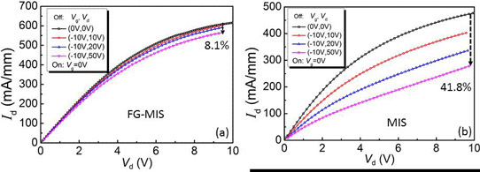
Figure 2: Output characteristics of (a) FG-MIS HEMT and (b) MIS HEMT with various off-state bias conditions, measured at 0V gate potential.
Fixed charges adversely impact channel mobility and are a factor in current collapse under pulsed operation (Figure 2). The off state was for a -10V gate potential and the on state was 0V. The off-state stress was varied up to a 50V drain bias. The devices were toggled on and off at 20-second intervals.
The on-state current with 10V drain bias was reduced by 41.8% with a 50V off-state stress in the conventional MIS-HEMT. The effect was reduced to 8.1% with the FG device. The researchers see the fixed interface charge of the non-FG transistor as trapping electrons that act as a ‘dummy gate’ and are slow to be released when the device is turned on.
The FG MIS-HEMT turned on faster than the conventional device and the on-state current was only slightly impacted by off-state drain bias as it increased to 100V. In addition to slower turn-on, the conventional MIS-HEMT saw a reduction of more than 2x in current as the off-state drain bias increased from 10V to 100V.
Fluorinated graphene AlGaN MIS-HEMTs AlGaN HEMT PECVD
https://doi.org/10.1109/LED.2017.2682261
The author Mike Cooke is a freelance technology journalist who has worked in the semiconductor and advanced technology sectors since 1997.


