


- News
24 April 2017
Alcohol-based digital etch on arsenide and antimonide III-V semiconductors
Massachusetts Institute of Technology (MIT) in the USA and IMEC in Belgium have developed digital etch (DE) techniques using alcohol solutions for III-V arsenide and antimonide semiconductors structures [Wenjie Lu et al, IEEE Electron Device Letters, published online 3 April 2017].
The researchers claim that their work represents the first demonstration of digital etch on the antimonide material system. Unfortunately, normal digital etch techniques are not suitable for antimonides since water constitutes an etchant in this material system, destroying the tight control needed for devices with small feature sizes.
Finally, gate-all-around nanowire metal-oxide-semiconductor field-effect transistors (MOSFETs) were produced using the alcohol-based digital etch. The work was supported by Samsung Electronics, the US Defense Threat Reduction Agency, the US NSF Center for Energy Efficient Electronics Science, Lam Research, and Korea Institute of Science and Technology.
Digital etch is seen as similar to atomic layer deposition (ALD), but in reverse. The technique consists of two self-limiting steps, giving fine control: 1, oxidation; and, 2. oxide removal. The oxidation step used by MIT was achieved through self-limiting oxygen plasma exposure in a barrel asher for 3 minutes. Removal was carried out by one of three wet techniques: 1. sulfuric acid in deionized (DI) water; 2. sulfuric acid (H2SO4) in methanol; or, 3. hydrochloric acid (HCl) in isopropanol (IPA). For antimonide semiconductors only the HCl:IPA removal solution could be used.
Samples consisting of indium gallium arsenide (In0.47Ga0.53As) and indium aluminium arsenide (In0.52Al0.48As) layers were grown by molecular beam epitaxy (MBE) on indium phosphide (InP) substrate. An antimonide (Sb) structure was also grown on GaAs substrate with 20nm of In0.28Ga0.72Sb on 200nm Al0.65Ga0.35Sb buffer.
The samples were prepared for digital etch by native oxide removal and the application of a 100nm hydrogen silsesquioxane (HSQ) mask on a 2nm silicon nitride adhesion layer. The HSQ was patterned using electron-beam lithography. Dry inductively coupled plasma etch gave fins or vertical nanowires (VNWs) of 230nm height.
The samples were prepared for digital etch by native oxide removal. For the arsenide sample, this was achieved by buffered oxide etch, which also removed the HSQ. Native oxide was removed from the antimonide layers by HCl:IPA solution, leaving the HSQ in place.
The effect of digital etch was analyzed by scanning electron microscopy (SEM). The radial etch rate for arsenide VNWs was 1.0nm/cycle for HCl:IPA solution and 1.2nm/cycle for H2SO4:methanol. The rate for H2SO4:DI water was 1.0nm/cycle.
An antimonide VNW was reduced from 100nm to 92nm diameter by exposure to DI water, showing its etching effect. The resulting surface was rough in the AlGaSb region. A similar effect was seen in antimonide fin structures. “Therefore, water-based DE is not viable for antimonides,” the researchers conclude.
The HCl:IPA digital etch on antimonide structures resulted in smoother sidewalls without excessive etching or surface damage. MIT estimates the etch rate of antimonide NWs to be 1.0nm/cycle.
Table 1: Mechanical yield of various diameter (D) InGaAs VNWs after 7 cycles of digital etch.
|
Dintial (nm) |
Dfinal (nm) |
DE:HCl/H2O Rinse:H2O |
DE:HCl/IPA Rinse:IPA |
DE:H2SO4/methanol Rinse:IPA |
DE:HCl/H2O Rinse:IPA |
| 28 | 14 | 100% | 100% | 100% | 100% |
| 26 | 12 | 31% | 100% | 100% | 100% |
| 24 | 10 | 5% | 100% | 100% | 0% |
| 22 | 8 | 0% | 97% | 95% | 0% |
| 20 | 6 | 0% | 5% | 90% | 0% |
The researchers also assessed mechanical yields. Surface tension in water-based processes are particularly damaging to thin VNW structures (Table 1). The team found 97% mechanical yield for 8nm arsenide VNWs thinned from 22nm diameter by 7-cycle HCl:IPA digital etch. By contrast, water-based processes gave 0% yield.
H2SO4:methanol digital etch allowed NWs of 6nm diameter to be reached with 90% yield, while HCl:IPA gave only 5%. According to the researchers: “This is likely due to the smaller viscosity of methanol (0.54cP) than that of IPA (2.0cP). These results indicate that NW breakage happens during the oxide etch process as well as while rinsing.”
The team adds: “It should be noted that 7 DE cycles is a harsh process that is typically unnecessary in actual device fabrication. In a shortened process, higher mechanical yields at smaller diameters should be possible.”
Previous digital etch work on arsenide VNWs has been limited to 11-15nm diameters, according to the researchers.
To test the electronic effectiveness of the 5-cycle H2SO4:methanol digital etch, the MIT team produced InGaAs VNW transistors (Figure 1). The gate stack consisted of 2nm aluminium oxide (1nm equivalent oxide thickness) and tungsten electrode. The ohmic source-drain contacts were molybdenum. The NW diameters were in the range 20-40nm. The channel was 80nm long.
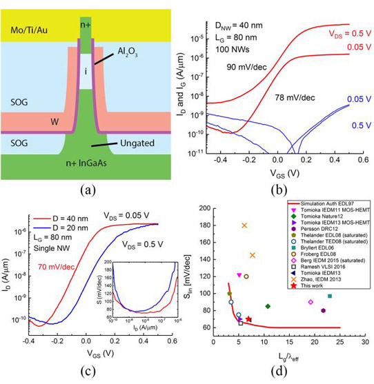
Figure 1: (a) Schematic cross section of InGaAs VNW-MOSFET; (b) subthreshold characteristics for transistor array with 100 40nm-diameter VNWs, treated with 5 DE cycles in H2SO4:methanol; (c) subthreshold characteristics of single 40nm-diameter VNW transistor with lowest linear swing of 70mV/decde. Inset: swing versus drain current. (d) Linear subthreshold swing versus ratio of gate length to natural length of InGaAs VNW MOSFETs.
The linear subthreshold swing of 40nm-diameter devices in an array of 100 NWs was 78mV/decade. A single NW transistor achieved a minimum of 70mV/decade. A 20nm-diameter NW transistor had a slightly higher swing of 74mV/decade with 0.5V drain bias. The researchers used the subthreshold characteristics to extract an estimate of the interface trap density at 3.9x10¹²/eV-cm2.
The team points out that the subthreshold swing remains below 80mV/decade over two orders of magnitude in drain current, adding: “This is one of the best linear subthreshold swings reported in InGaAs VNW-MOSFETs.”
https://doi.org/10.1109/LED.2017.2690598
The author Mike Cooke is a freelance technology journalist who has worked in the semiconductor and advanced technology sectors since 1997.


