


- News
6 April 2017
Direct growth of III-V material on silicon for 1.55μm quantum dot lasers
Hong Kong University of Science and Technology (HKUST) and Harvard University in the USA have reported progress on direct epitaxy of III-V quantum dot (QD) materials on silicon, producing 1.55μm microdisk lasers (MDLs) [Bei Shi et al, Appl. Phys. Lett., vol110, p121109, 2017].
The 1.55μm wavelength is used in long-distance telecommunications over low-attenuation optical fibers. Normally such devices are grown on indium phosphide (InP). Electrically driven III-V quantum dot laser materials on silicon have recently been realized for shorter, non-optimal 1.3μm wavelengths.
Integrating lasers with silicon would allow more compact and versatile low-cost silicon photonics with applications covering on-chip optical communications and data processing, along with biological sensing. The HKUST/Harvard team sees their work as “a promising path towards large-scale integration of cost-effective and energy-efficient silicon-based long-wavelength lasers.”
Quantum dots are seen as a way to lower laser thresholds, improved thermal stability, and increased robustness against the effects of defects.
The III-V material was all grown on (001) silicon using metal-organic chemical vapor deposition (MOCVD). A number of strategies were deployed to reduce threading dislocations, anti-phase boundaries, and other common defects arising from the 8% mismatch between the InP and Si crystal lattices (Figure 1):
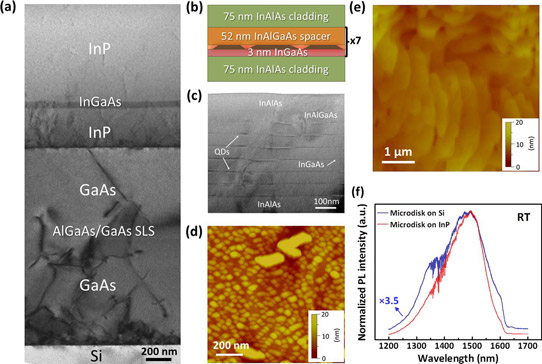
Figure 1: (a) Cross-sectional transmission electron microscope (TEM) image of InP/Si template; (b) schematic of microdisk laser structure; (c) close-up TEM of the microdisk laser on Si, highlighting InAs/InGaAs/InAlGaAs DWELLs; (d) representative surface morphology of uncapped InAs QDs on top of InP/Si substrate; (e) typical 5μmx5μm AFM image of InP thin-film surface grown on Si; (f) room-temperature photoluminescence of as-grown microdisk laser material on Si and InP substrates, respectively.
1. A 1.7μm gallium arsenide (GaAs) intermediate buffer to accommodate the InP/Si mismatch. The GaAs buffer incorporated an aluminium gallium arsenide (AlGaAs)/GaAs strained-layer superlattice (SLS) to reduce dislocation densities and give a smooth surface.
2. The InP buffer layer was grown in stages, starting with 70nm low-temperature nucleation and continuing with 1.4μm of InP buffer grown in multiple temperature steps. The InP buffer included a 60nm In0.6Ga0.4As strained-interlayer designed to filter dislocations from the GaAs/InP interface.
The resulting InP/Si template surface had 1.6nm root-mean-square roughness, according to 5μmx5μm atomic force microscopy (AFM).
The microdisk laser structure consisted of a 7-period quantum dot in well (DWELL) structure sandwiched between 75nm InAlAs cladding layers. The InAs quantum dots had 45nm typical diameter with 4x10¹⁰/cm2 density. The 3nm InGaAs served as a wetting layer. The InAlGaAs was applied in two steps – 1.5nm low-temperature material to avoid desorption of the underlying dots, and a 52nm high-temperature spacer layer. The high temperature also annealed the dots to prevent dot-height dispersion and to tune the emission wavelength.
Comparing the photoluminescence (PL) with material grown on InP substrates showed a factor of 3.5 lower emission from the structure grown on the InP/Si template. The emission line was broader and a shoulder was present in the latter material. The researchers suggest that this could be due to dot-size fluctuation. They add: “The broad spectra however favor the interaction between resonant modes in small cavities and the material gain.”
The lasers consisted of 1.5μm-diameter microdisks formed by colloidal lithography and dry etching down to the InP buffer. A selective wet etch then formed an InP pillar.
The laser was pumped using a 532nm Q-switched neodymium-doped yttrium aluminium garnet (Nd:YAG) pulsed laser source (20ns pulse width, 3000Hz repetition rate). Stimulated emission with a 1563nm wavelength was achieved with a high background suppression ratio of 21.7dB. There was some increase in linewidth above threshold, attributed to wavelength chirping from changes in refractive index caused by transient changes of carrier density in the QDs.
The threshold pumping power was 2.73±0.23μW. The researchers say that this is an upper bound, since no account was taken of multiple reflection/absorptions inside the disk and coupling efficiency of the pump beam.
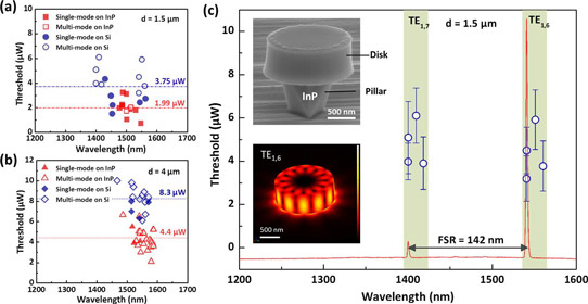
Figure 2: Single-mode (solid symbols) and multi-mode (open symbols) lasing threshold dispersion of (a) 1.5μm and (b) 4μm microdisks on InP and Si as function of wavelength; (c) Overlay of threshold powers in multi-mode 1.5μm disks with representative lasing spectrum. Top inset: scanning electron microscope image; bottom inset: three-dimensional electric field distribution of simulated TE{1,6} mode.
Statistical studies with various 1.5μm and 4μm disk diameters demonstrated thresholds for devices on In/Si templates about twice that of lasers produced on pure InP substrates (Figure 2). The team comments: “The larger thresholds on silicon are mainly associated with three factors. First, the material gain in the QD active region on silicon is somewhat lower due to non-radiative recombination processes introduced by crystalline defects. Second, the injection efficiency is reduced because the pump laser generated carriers can be partially trapped by the deep energy level traps related with dislocations in the disk region. Moreover, the broader PL emission spectrum of the MDL on silicon is more favorable for multi-mode lasers.”
Varying the temperature up to 60°C, the researchers extracted a high threshold characteristic (T0) of 123K for one mode (TE{1,6}, 1546.9nm). They describe this value as “among the best reported T0 for QD MDLs on III-V substrates.” The other mode studied (TE{1,7}, 1406.2nm) had a lower T0 of 90K. The team comments: “the larger T0 of the TE{1,6} mode can be attributed to a better overlap with the gain spectrum at higher temperatures and a superior carrier capture efficiency in larger QDs, which prevent carrier evaporation into barriers.”
Direct epitaxy of III-V quantum dot materials on silicon Microdisk lasers MOCVD
http://dx.doi.org/10.1063/1.4979120
The author Mike Cooke is a freelance technology journalist who has worked in the semiconductor and advanced technology sectors since 1997.


