


- News
21 October 2016
First 1.3μm electroluminescence from MOCVD quantum dots on silicon
The University of Tokyo in Japan claims "the first demonstration of electroluminescence (EL) at 1.3μm from InAs/GaAs quantum dots (QDs) monolithically grown on a Ge/Si substrate by metal organic chemical vapor deposition (MOCVD)" [Mohan Rajesh et al, Jpn. J. Appl. Phys., vol55, p100304, 2016].
The researchers see the room-temperature achievement as an important milestone towards the monolithic integration of indium arsenide/gallium arsenide (InAs/GaAs) QD lasers emitting at 1.3μm for silicon photonics application.
QD lasers can have improved characteristics such as low threshold current and high temperature stability compared with more traditional devices based on quantum wells. Producing electrically pumped lasers on silicon could plug the light generation gap in silicon photonics technologies for data communications and high-speed computer processing. QD lasers have been produced through molecular beam epitaxy (MBE) on silicon, but MOCVD is often a preferred mass-production technology in terms of high throughput and low maintenance cost.
The Tokyo indium arsenide in gallium arsenide matrix (InAs/GaAs) QD structures were produced on a germanium (Ge) interlayer on the silicon (Si) substrate. III-V material such as GaAs tends to suffer from crystal imperfection when grown directly on Si due to a large 4.1% lattice mismatch. Germanium has a smaller mismatch with GaAs of the order of 0.07%. Also the thermal expansion coefficients of Ge and GaAs are similar, an important factor when high-temperature growth processes are used.
The 2μm Ge interlayer was grown using ultra-high-vacuum CVD on 6°-offcut silicon substrate. A further 100nm of Ge was grown after 5 minutes of cyclic annealing at 850°C. The Ge/Si wafer was prepared for III-V MOCVD by a series of treatments to remove contaminants and native oxide.
When the Ge/SI wafer was loaded into the MOCVD reactor a further treatment of thermal annealing in tertiarybutylarsine at 650°C for 10 minutes was used to desorb native oxide and create double atomic steps on the substrate surface, avoiding antiphase domains (APDs) in the subsequent growth.
The GaAs buffer layer consisted of 10nm nucleation on the As pre-layer at 420°C, 250nm low-temperature 500°C material, and finally the main part at 650°C to give 1.3μm or 3μm total thickness. The lower-temperature layers used triethylgallium precursor, while the high-temperature final part used trimethylgallium. Before QD deposition, the GaAs/Ge/Si wafer was annealed in tertiarybutylarsine.
The QDs were grown in a series of layers using antimony (Sb) as a surfactant. The Sb was irradiated onto the GaAs surface, after which the 3.8-monolayer InAs QD material was deposited at 495°C. The growth was then interrupted for 80 seconds. The QD density was greater than 4.3x10¹⁰/cm2. The base width and height were 36nm and 7nm, respectively. "The density of QDs grown on GaAs/Ge/Si substrate is almost comparable to that of QDs grown on a GaAs substrate, used for the fabrication of low-threshold-current lasers," the team writes.
The QD layer was capped with 500°C 7nm In0.05Ga0.95As and 5nm GaAs. The purpose of the In0.05Ga0.95As layer was to reduce strain and to red-shift the InAs QD emission wavelength to 1.3μm and longer with a full-width at half-maximum (FWHM) of ~44meV. The QD layers were completed with a 600°C 30nm GaAs spacer for the next QD layer.
The antimony surfactant-mediated growth increases dot density and suppresses coalescence. With certain growth conditions it can also increase photoluminescence (PL) intensity. Previous work on InAs/GaAs QD MOCVD on germanium substrates has resulted in low densities and coalescence of dots.
It was found that the GaAs buffer layer (BL) needed to be annealed at 600°C to give photoluminescence intensity comparable with QDs grown on GaAs substrate.
The researchers comment: "The lower PL intensity in the case of QDs grown on a Ge/Si substrate may be attributed to the relaxation of charge carriers to non-radiative recombination centers, such as threading dislocations and APDs, formed at the GaAs/Ge interface and propagating into the GaAs BL and reaching the QD active region, thereby quenching the QD emission efficiency. We have observed that the post-growth thermal annealing of the GaAs buffer layer prior to the growth of QDs can be a simple and effective tool for improving the luminescence efficiency of the QDs grown on Ge/Si substrates."
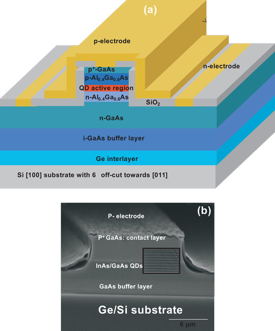
Figure 1. (a) Schematic layer structure of InAs/GaAs QD LED grown on Ge/Si substrate. (b) Cross-sectional high-resolution scanning electron microscope image of fabricated device.
The researchers used these techniques to create light-emitting diodes (LEDs) with eight layers of QDs (Figure 1). The n- and p-cladding layers consisted of 1.4μm Al0.4Ga0.6As. These layers were grown at more than 600°C, which can degrade underlying QDs in the case of the p-type cladding. In particular, the high temperature can diffuse gallium into and indium out of the dots, shortening the wavelength of emissions.
The researchers comment: "The realization of EL at 1.3μm on Ge/Si, which is not blue-shifted, is attributed to our improved growth conditions of the InAs/Sb:GaAs QDs in the active layer, particularly the Sb irradiation time, before the deposition of InAs, as InAs/Sb:GaAs QDs do not show any blue-shift upon annealing at temperatures as high as 630°C."
The structure was capped with a 300nm p+-GaAs contact. The contact metal electrodes were gold on gold-germanium-nickel alloy. The electron current injection was lateral from the top side of the device to avoid added series resistance from the high-defect-density GaAs/Ge/Si interfaces.
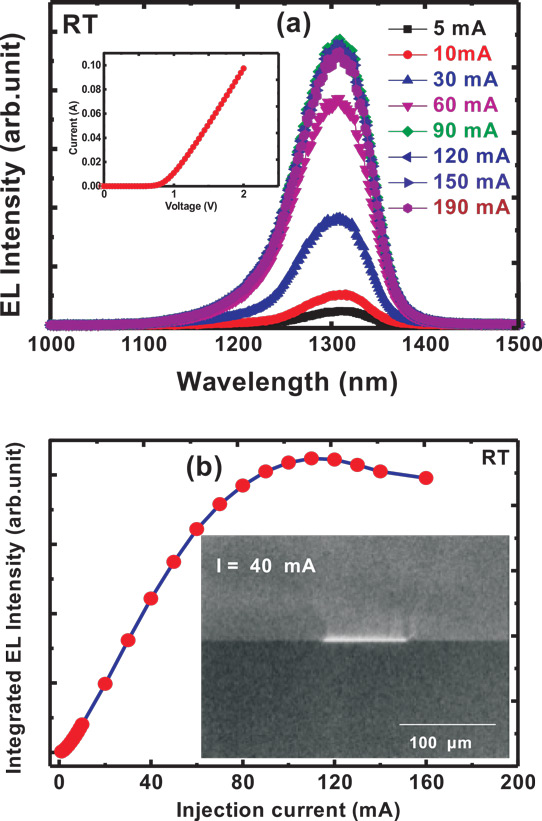
Figure 2. (a) EL spectra of device at room temperature at various injection currents. Inset: current-voltage characteristics of diode. (b) Integrated EL intensity as function of injection current. Inset: infrared camera near-field image of light emission from as-cleaved facet bar at 40mA.
Under reverse bias the current was of the order 10-8A, suggesting a good rectifying pn junction. Electroluminescence turned on around +0.8V forward bias (Figure 2). Series resistance was around 10Ω. The peak wavelength was 1.3μm with 54meV full-width half-maximum.
The researchers comment: "To the best of our knowledge, this is the first demonstration of EL at 1.3μm from III–V QDs directly grown on a Ge/Si substrate by MOCVD."
Below 80mA, the increase in intensity with current is approximately linear. With further injection, the output saturates around 130mA and then falls back slightly due to thermal roll-over, non-radiative Auger processes, etc.
The output suffers from imperfect facets from non-parallel/non-vertical cleavage along the [100] plane. "The combined effect of facet polishing and high-reflection coating on the facets apart from further improving the uniformity of the QDs in the active region and reducing the defect density in the buffer layer could potentially lead to the realization of a QD laser on Si by MOCVD," the team believes.
http://doi.org/10.7567/JJAP.55.100304
The author Mike Cooke is a freelance technology journalist who has worked in the semiconductor and advanced technology sectors since 1997.


